SiC/Si heterojunction lateral photosensitive IMPATT diode and preparation method thereof

A diode and heterojunction technology, which is applied in the field of SiC/Si heterojunction lateral photosensitive IMPATT diodes and their preparation, can solve the problems of difficult monolithic integration of diodes, difficult to achieve control of diode performance, etc. Effect

Active Publication Date: 2019-03-22
WENZHOU UNIVERSITY
View PDF5 Cites 4 Cited by
  • Summary
  • Abstract
  • Description
  • Claims
  • Application Information

AI Technical Summary

Problems solved by technology

These axial n + -n-p-p + The structure of type IMPATT and MITATT diodes is easy to manufacture, but it is difficult to couple light into the avalanche generation region of the device, and the photogenerated carriers are not easy to mix with the carriers generated by avalanche, so it is difficult to realize the control of light on the performance of IMPATT and MITATT diodes
In addition, the axial n + npp + Type IMPATT, MITATT diodes are difficult to monolithically integrate, and special complex technology is required to connect the axial IMPATT, MITATT diodes in series to synthesize the power combination circuit
[0004] The recently developed Si / 3C-SiC heterojunction shows excellent application prospects [Li L.B., et al., Materials Letters, 2016,163(1):47-50.], axial 3C-SiC / Si heterojunction Junction lateral photosensitive IMPATT diodes have better large-signal performance than Si homojunction devices at frequencies of 0.3THz and 0.5THz [Banerjee S., et al., Progress in Electromagnetics Research Symposium, Stockholm, Sweden, 2013: 462- 466.], but there is no report on SiC / Si heterojunction lateral photosensitive IMPATT diode

Method used


Image

  • SiC/Si heterojunction lateral photosensitive IMPATT diode and preparation method thereof
  • SiC/Si heterojunction lateral photosensitive IMPATT diode and preparation method thereof
  • SiC/Si heterojunction lateral photosensitive IMPATT diode and preparation method thereof

Examples


Embodiment Construction

[0044] In order to make the object, technical solution and advantages of the present invention more clear, the present invention will be further described in detail below in conjunction with the accompanying drawings and embodiments. It should be understood that the specific embodiments described here are only used to explain the present invention, not to limit the present invention.

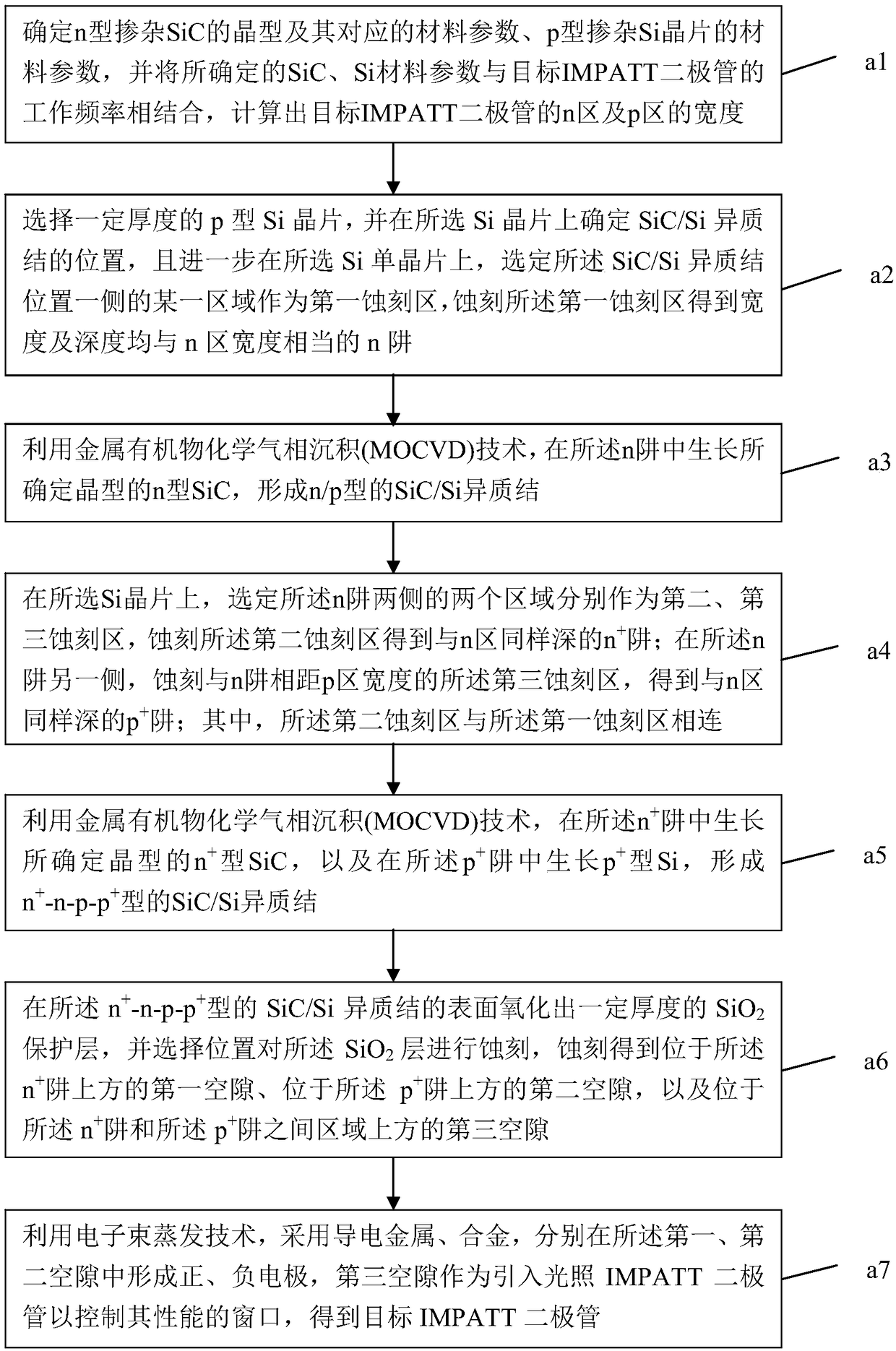
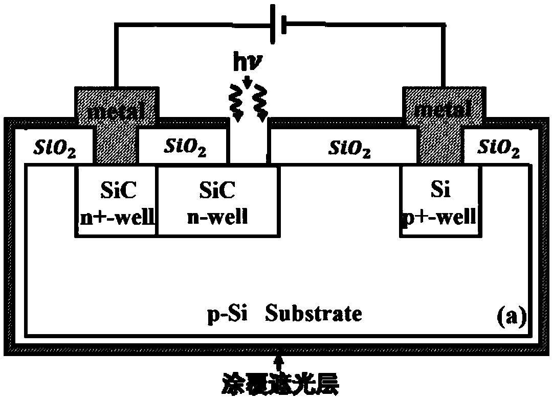
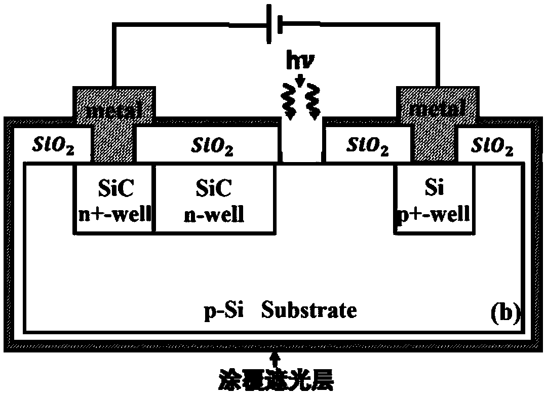
[0045] Such as figure 1 As shown, in Embodiment 1 of the present invention, a method for preparing a SiC / Si heterojunction lateral photosensitive IMPATT diode is provided, and the method includes the following steps:

[0046] Step a1, determine the crystal form of n-type doped SiC and its corresponding material parameters, and the material parameters of p-type doped Si wafer, and combine the determined SiC and Si material parameters with the operating frequency of the target IMPATT diode to calculate Get the n-type region and p-type region width of the target IMPATT diode;

[0047] Step a2, se...


PUM


Abstract

The invention discloses a SiC/Si heterojunction lateral photosensitive IMPATT diode and a preparation method thereof. The preparation method comprises the steps of: firstly, determining an SiC crystalform and material parameters, combining a working frequency of a target IMPATT diode, and calculating widths of an n-type region and a p-type region; secondly, selecting a p-type Si single crystal wafer of a certain thickness, preparing an n well, an n+ well and a p+ well in the selected Si single crystal wafer respectively according to the widths of the n-type region and the p-type region, and growing the crystal form SiC in the n well and the n+ well; thirdly, preparing an SiO2 protective layer through oxidization, coating a light shielding layer of an appropriate thickness thereon, and etching first and second gaps which form electrodes and a third gap which is used for introducing illumination to regulate and control performance of the IMPATT diode; and finally generating electrodes to obtain the target IMPATT diode. The SiC/Si heterojunction lateral photosensitive IMPATT diode and the preparation method thereof have the advantages of monolithic integration and series combination,and are prone to realize the entrance of illumination into an avalanche region of the IMPATT diode to affect its performance.

Description

technical field [0001] The invention relates to the technical field of electronic transistors, in particular to a SiC / Si heterojunction lateral photosensitive IMPATT (Impact Avalanche and Transist-Time) diode and a preparation method thereof. Background technique [0002] Silicon carbide (SiC) has an indirect band gap semiconductor than silicon (Si), and SiC has a higher band gap than Si, a higher critical breakdown field strength, a faster carrier saturation drift speed and a higher Excellent thermal conductivity, more suitable for high frequency and high power IMPATT diodes. The SiC / Si heterojunction can take advantage of the mutual advantages of the two materials and make up for their respective defects, which can be used to improve the performance of semiconductor devices. [0003] For example, the literature [Ghosh M., et al., Journal of Computational Electronics, 2016,15(4):1370-1387.] simulated that the avalanche generation region is Si / 3C-SiC multiple quantum wells,...

Claims


Application Information

Patent Timeline
Patent Type & Authority Applications(China)
IPC IPC(8): H01L31/107H01L31/0336H01L31/18
CPCH01L31/0336H01L31/1075H01L31/1804Y02P70/50
Inventor 韦文生林宇豪
Owner WENZHOU UNIVERSITY
Why Eureka
Try Eureka