Method of growing high-quality gallium nitride film on silicon substrate

A high-quality gallium nitride technology, applied in electrical components, semiconductor/solid-state device manufacturing, circuits, etc., can solve the problems of GaN cracks and other problems, and achieve the effect of high-quality crack-free GaN thin film epitaxial growth

Inactive Publication Date: 2019-03-26
江苏晶曌半导体有限公司
View PDF5 Cites 7 Cited by
  • Summary
  • Abstract
  • Description
  • Claims
  • Application Information

AI Technical Summary

Problems solved by technology

However, GaN is directly grown on the AlN film by high-temperature epitaxial growth, and the residual compressive stress is only 15% of the theoretical value, so if there is no good stress control method, GaN is extremely prone to cracks

Method used


Image

  • Method of growing high-quality gallium nitride film on silicon substrate
  • Method of growing high-quality gallium nitride film on silicon substrate
  • Method of growing high-quality gallium nitride film on silicon substrate

Examples


Embodiment 1

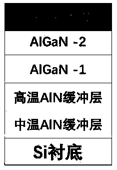
[0022] This embodiment provides a method for growing a high-quality gallium nitride film on a silicon substrate, which is carried out in an MOCVD device, using TMAl, TMGa, NH 3 As Al source, Ga source and N source respectively, H 2 as a carrier gas. The method for growing a high-quality gallium nitride thin film on a silicon substrate in this embodiment includes the following steps:

[0023] (1-1) Dry the purchased 800 μm thick Si substrate (Si(111)) and place it on the N 2 In the MOCVD glove box with a protective atmosphere, the substrate was then moved to the substrate tray in the MOCVD reaction chamber using a suction cup, and the surface temperature of the epitaxial wafer was raised to 1050 °C in a hydrogen atmosphere, and the surface oxide was removed by heat treatment for 5 minutes;

[0024] (1-2) Cool down the reaction chamber to 1000°C, first pass TMAl for 12s, the flow rate is 72 μmol / min, and then pass NH 3 , the flow rate is 0.12 mol / min, the pressure is 100 mbar...

Embodiment 2

[0032] This embodiment provides a method for growing a high-quality gallium nitride film on a silicon substrate, which is carried out in an MOCVD device, using TMAl, TMGa, NH 3 As Al source, Ga source and N source respectively, H 2 as a carrier gas. Specifically include the following steps:

[0033] (2-1) Place the purchased 800 μm thick Si substrate (Si(111)) in the MOCVD glove box after drying, and then use the suction cup to move the substrate to the substrate tray in the MOCVD reaction chamber, under the hydrogen atmosphere Raise the surface temperature of the epitaxial wafer to 1060°C, heat treatment for 5 minutes to remove the surface oxide;

[0034] (2-2) Cool down the reaction chamber to 980°C, first pass TMAl for 15s, the flow rate is 78 μmol / min, and then pass ammonia NH 3 , the flow rate is 0.10 mol / min, the pressure is 100 mbar, and the medium temperature AlN core layer is deposited on the Si substrate with a thickness of 30 nm;

[0035] (2-3) Raise the tempera...

Embodiment 3

[0041] This embodiment provides a method for growing a high-quality gallium nitride film on a silicon substrate, which is carried out in an MOCVD device, using TMAl, TMGa, NH 3 They are respectively used as Al source, Ga source and N source, and H2 is used as carrier gas. Specifically include the following steps:

[0042] (3-1) Dry the purchased Si substrate (Si(111)) with a thickness of 800 μm and place it in the MOCVD glove box, then use the suction cup to move the substrate to the substrate tray in the MOCVD reaction chamber. Raise the surface temperature of the epitaxial wafer to 1080°C, heat treatment for 3 minutes to remove the surface oxide;

[0043] (3-2) Cool down the reaction chamber to 1000°C, first pass TMAl for 10s, the flow rate is 75μmol / min, and then pass NH 3 , the flow rate is 0.10mol / min, the pressure is 100mbar, and the medium temperature AlN core layer is deposited on the Si substrate with a thickness of 40nm;

[0044] (3-3) Raise the temperature in the...


PUM

PropertyMeasurementUnit
thicknessaaaaaaaaaa
thicknessaaaaaaaaaa

Abstract

The invention provides a method of growing a high-quality gallium nitride film on a silicon substrate. The method comprises the following steps: (1), performing oxide removal operation on a Si substrate; (2), depositing AlN buffer layers including a low-temperature AlN buffer layer and a high-temperature AlN buffer layer on the Si substrate; (3), depositing a AlGaN-1 buffer layer on the high-temperature AlN buffer layer; (4), depositing a AlGaN-2 buffer layer on the AlGaN-1 buffer layer; and (5), growing a GaN epitaxial layer on the AlGaN-2 buffer layer. According to the invention, on the basis of the AlGaN / AlN epitaxial structure, the compressive stress is introduced in advance to enable the epitaxial wafer to protrude; during the cooling process after GaN growth completion, the GaN filmshrinks faster than the Si substrate and the GaN-Si epitaxial wafer changes from the convex shape to a non-warped shape. According to the invention, with the two AlGaN buffer layers, the high-qualitycrack-free GaN film epitaxial growth is realized.

Description

technical field [0001] The invention belongs to the technical field of LED chip epitaxial growth, and in particular relates to a method for growing a high-quality gallium nitride thin film on a silicon substrate. Background technique [0002] Compared to Al 2 o 3 , SiC or GaN substrates, Si substrates are the preferred substrates for GaN-based HEMT epitaxial growth due to their advantages of low price, easy preparation of large sizes and compatibility with traditional silicon processes. However, since the Si(100) plane atoms are not hexagonally symmetrical, it is extremely difficult to epitaxially grow high-quality hexagonal nitride films on Si(100) substrates, and there is a large lattice mismatch between the GaN epitaxial layer and the silicon substrate. Due to the thermal mismatch, the grown GaN epitaxial layer is subject to a great tensile stress, resulting in high-density cracks, dislocations, and large warpage of the substrate in the epitaxial layer. Due to the stro...

Claims


Application Information

Patent Timeline
Patent Type & Authority Applications(China)
IPC IPC(8): H01L21/02
CPCH01L21/02389H01L21/0254
Inventor 白俊春周小伟景文甲李培咸平加峰
Owner 江苏晶曌半导体有限公司
Why Eureka
Try Eureka