Organic electroluminescence device and display device

An electroluminescence device and electroluminescence technology, which are applied in the fields of electro-solid devices, electrical components, semiconductor devices, etc., can solve the problems of low luminous efficiency and low life of the device, and achieve improved luminous efficiency, good energy level matching, and improved Effect of Luminous Efficiency and Lifespan

Inactive Publication Date: 2019-03-26
YUNGU GUAN TECH CO LTD
View PDF9 Cites 5 Cited by
  • Summary
  • Abstract
  • Description
  • Claims
  • Application Information

AI Technical Summary

Problems solved by technology

[0004] However, in the thermally activated delayed fluorescence devices at the present stage, there are often situations where the device luminous efficiency is low and the lifetime is low.

Method used


Image

  • Organic electroluminescence device and display device
  • Organic electroluminescence device and display device
  • Organic electroluminescence device and display device

Examples


Embodiment 1-11

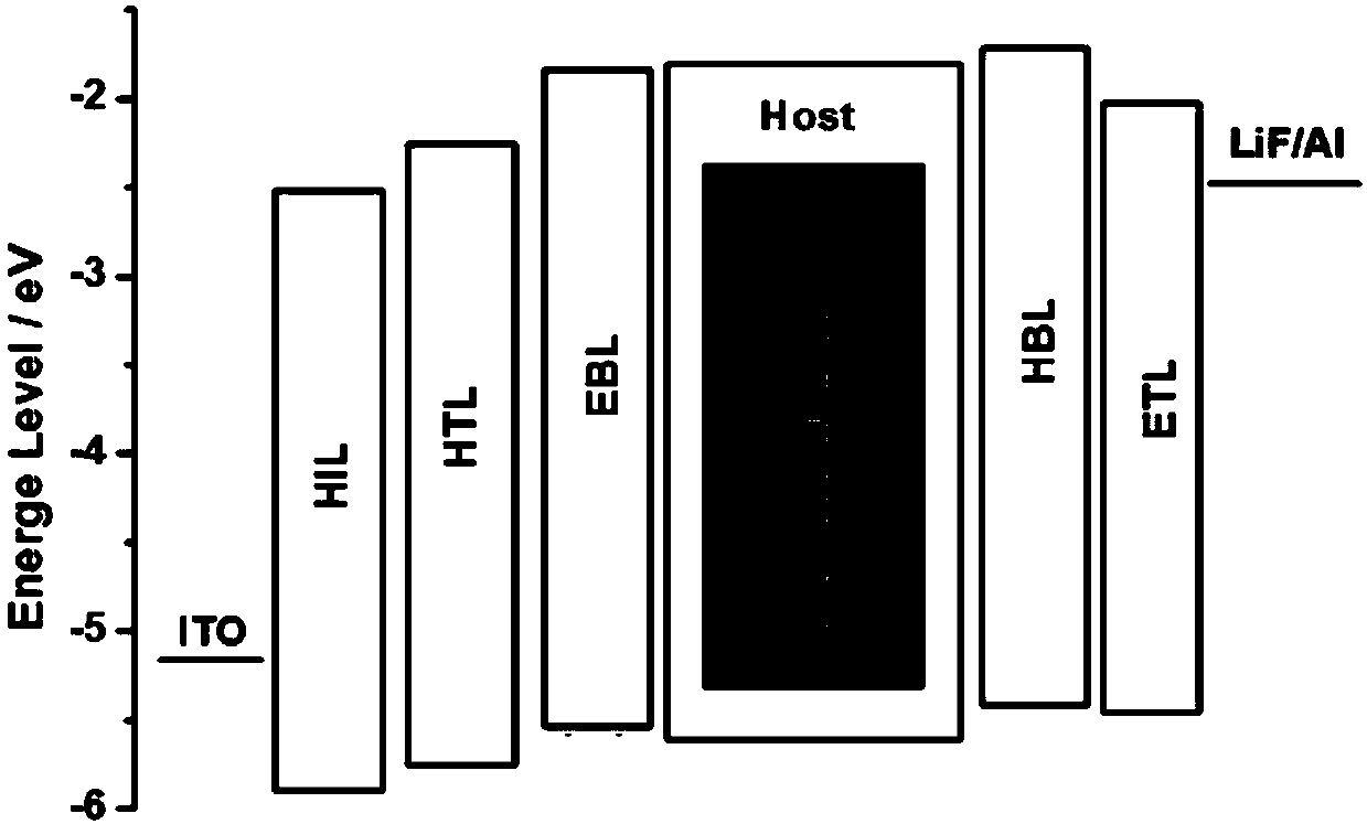
[0066] Such as image 3 As shown, each of Examples 1-11 provides an organic electroluminescent device, which in turn includes an anode, a hole injection layer (HIL), a hole transport layer (HTL), an electron blocking layer (EBL), and a light emitting layer (EML) , Hole blocking layer (HBL), electron transport layer (ETL), electron injection layer (EIL) and cathode.

[0067] Among them, the device structure of embodiment 1 is: ITO / HATCN (10nm) / NPB (40nm) / electron blocking (5nm) / body: 30% T-76: 5% F-8 (30nm) / hole blocking (5nm) ) / TPBI(30nm) / LiF(1nm) / Al(200nm).

[0068] The device structure of Examples 2-11 is basically the same as that of Example 1, except that the materials of the light-emitting layer, the hole blocking layer, and the electron blocking layer are different.

[0069] In the organic electroluminescent devices provided in Examples 1-11, the specific selection and doping concentration of the materials of the light-emitting layer, the hole blocking layer and the electron ...

Embodiment 12-15

[0091] Such as image 3 As shown, Examples 12-15 respectively provide an organic electroluminescent device. The device structure is basically the same as that of Example 1. The only difference is that the doping concentration of the sensitizer in the light-emitting layer is different. The doping concentration and the test results of the corresponding organic electroluminescent devices are shown in Table 3.

[0092] table 3

[0093]

[0094] From the test results in Table 3 in combination with Table 2, it can be seen that as the doping concentration of the TADF material as the sensitizer in the light-emitting layer changes, the luminous efficiency and service life of the corresponding OLED device also change. When the doping concentration of the TADF material in the light-emitting layer is 5-40 wt%, the OLED device has relatively best luminous efficiency and service life. In particular, when the doping concentration of the TADF material is 30 wt%, the performance of the OLED devic...

Embodiment 16-19

[0097] Such as image 3 As shown, Examples 16-19 respectively provide an organic electroluminescent device. The device structure is basically the same as that of Example 2, except for the thickness of the hole blocking layer. The thickness of the hole blocking layer in specific examples 16-19 and the test results of the corresponding organic electroluminescent devices are shown in Table 4.

[0098] Table 4

[0099]

[0100] It can be seen from Table 4 in combination with the test results of the foregoing Examples 1-15 that when TADF material is used as the sensitizer in the light-emitting layer, and both the hole blocking layer and the electron blocking layer contain TADF material, the thickness of the hole blocking layer increases with Change, the luminous efficiency and service life of OLED devices have changed. When the thickness of the hole blocking layer is 1-100nm, especially 1-50nm, the luminous efficiency of the OLED device is relatively high and the lifetime is relativel...


PUM


Abstract

The invention provides an organic electroluminescence device and a display device. The organic electroluminescence device comprises a light-emitting layer, a hole blocking layer and an electron blocking layer, wherein the material of the light emitting layer comprises a main material, a guest material and a first thermal activation delay fluorescent material; the material of the hole blocking layer comprises a second thermal activation delay fluorescent material; the material of the electron blocking layer comprises a third heat-activated delay fluorescent material. According to the invention,the TADF material is adopted as a sensitizing agent in the light-emitting layer. In the hole blocking layer and the electron blocking layer, the TRGB material is used at the same time, so that the luminous efficiency of the organic electroluminescent device can be improved, and the service life of the organic electroluminescent device can be prolonged.

Description

Technical field [0001] The invention belongs to the field of display technology, and specifically relates to an organic electroluminescence device and a display device. Background technique [0002] The organic electroluminescent device is provided with a light-emitting layer between the electron transport layer and the hole transport layer, and further set a cathode and an anode on the side of the electron transport layer and the hole transport layer away from the light-emitting layer, and apply a voltage to the device It is a device that injects electrons and holes and recombines to form excitons in the light-emitting layer, and emits photons outward through the process of fluorescence or phosphorescence. Because of its all-solid-state, self-luminous, wide viewing angle, fast response speed, low driving voltage, low energy consumption and many other characteristics, it has huge application prospects in the display and lighting fields. [0003] In recent years, Thermally Activate...

Claims


Application Information

Patent Timeline
Patent Type & Authority Applications(China)
IPC IPC(8): H01L51/50H01L51/54
CPCH10K50/121H10K50/18H10K50/11H10K2101/10
Inventor 李国孟徐超魏金贝李梦真
Owner YUNGU GUAN TECH CO LTD
Why Eureka
Try Eureka