An artificial surface plasmon radiator and control method based on f-p cavity loading
An artificial surface plasmon and F-P technology, applied in the field of vacuum electronics, can solve problems such as difficult to achieve super radiation, difficult to achieve, complex structure, etc.
- Summary
- Abstract
- Description
- Claims
- Application Information
AI Technical Summary
Problems solved by technology
Method used
Image
Examples
Embodiment 1
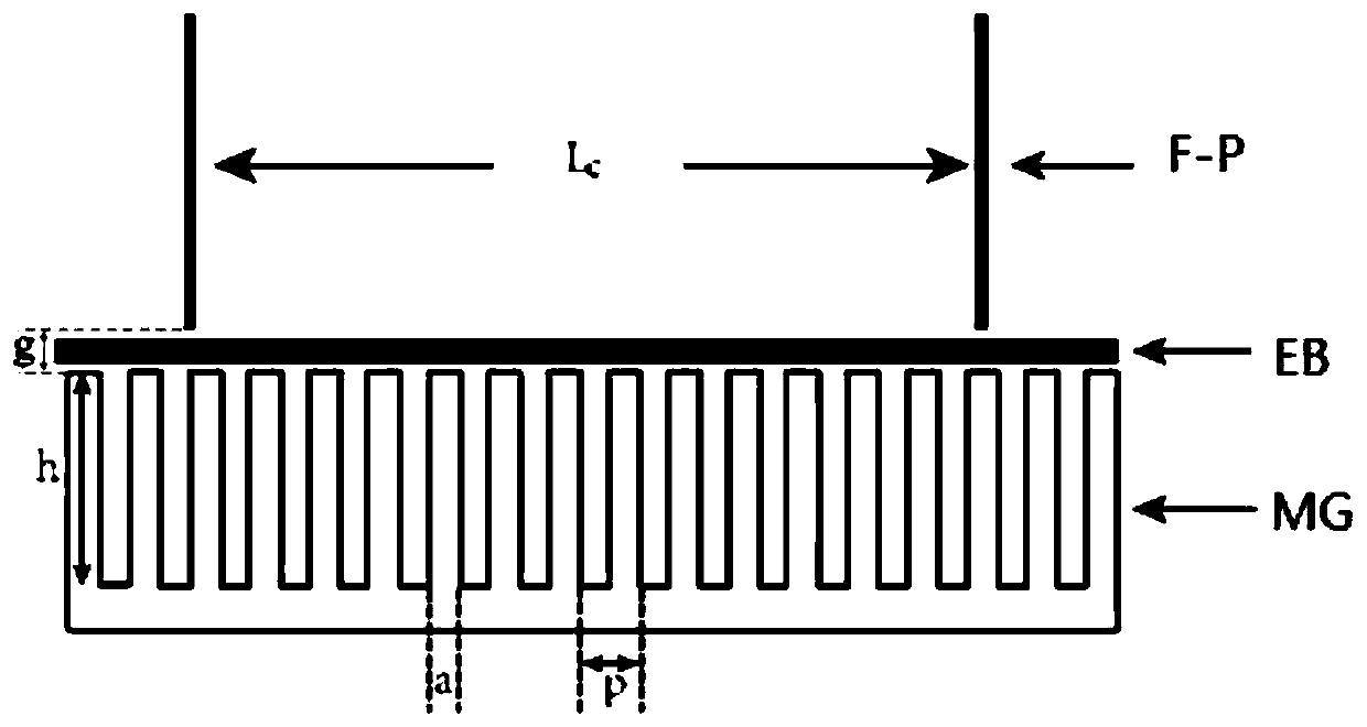
[0040] Such as figure 1 As shown, the artificial surface plasmon radiator based on the F-P cavity loading of the present embodiment includes: a metal grating and a Fabry-Perot F-P cavity; wherein, a Fabry-Perot F-P cavity is set above the metal grating ; The gap between the F-P cavity and the metal grating is g, less than the attenuation distance of the SSP perpendicular to the direction of the metal grating, and greater than or equal to the width of the electron beam; the unit period length of the metal grating is p, the metal width is a, and the groove depth is h; The Fabry-Perot F-P cavity includes first and second mirrors with length L c ; The electron beam passes through the gap between the F-P cavity and the metal grating, the SSP is excited on the surface of the metal grating, the working voltage of the electron beam is U, and the current is I.
[0041] In this embodiment, p=20 μm, a=10 μm, h=69 μm, the gap between the F-P cavity and the grating g=5 μm, and the cavity ...
Embodiment 2
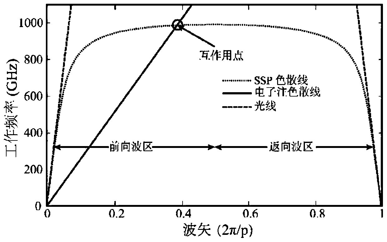
[0049] In this embodiment, the structure is the same as the first embodiment, the interaction point is located in the forward wave region, the working voltage U=3kV of the electron beam, and the current I=20mA.
[0050] The control method of the artificial surface plasmon radiator based on F-P cavity loading in this embodiment includes the following steps:
[0051] 1) Design structural parameters;
[0052] 2) According to the unit period length, metal width and groove depth of the metal grating, the dispersion line of the metal grating is obtained, and the wave loss and frequency corresponding to the midpoint of the dispersion line are obtained. The area before the midpoint of the dispersion line is the forward wave The area after the midpoint of the dispersion line is the backward wave area; the dispersion line of the electron beam is obtained according to the operating voltage of the electron beam; the intersection point of the dispersion line of the electron beam and the di...
PUM
 Abstract
Description
Claims
Application Information


