Laser processing chip method and device

A laser processing and chip technology, used in laser welding equipment, metal processing equipment, manufacturing tools, etc., can solve the problems of uneven groove depth and width, damage to the bottom readout circuit, and affect the effective pixel area area. Reduce the influence of groove width and depth uniformity, improve the effect and chip reliability, and improve the effect of pixel utilization

Active Publication Date: 2019-03-29
北京中科镭特电子有限公司
View PDF8 Cites 0 Cited by
  • Summary
  • Abstract
  • Description
  • Claims
  • Application Information

AI Technical Summary

Problems solved by technology

The advantages of this method: simple operation, low equipment requirements, and good etching selectivity; disadvantages: first, a photolithography process is required for each chip, which is time-consuming and laborious; Liquid, complex corrosion process, low precision, easy to damage the bottom readout circuit
The advantages of dry etching: the first etching selectivity and anisotropy are good, the second etching pattern can be precisely controlled and the resolution is high; the disadvantages: first, a single chip needs to be photolithography, which is time-consuming and laborious, and the second is damage Bottom readout circuit
[0007] At the same time, in the prior art, when the galvanometer is used to control the relative movement of the laser spot and the detector chip through the laser grooving method, due to the limitation of the galvanometer control method, when the square-shaped grooving is performed to form a closed annular groove, the corner There will be an arc at the corner, resulting in uneven depth and width of the groove at the corner, and affecting the area of ​​the effective pixel area

Method used


Image

  • Laser processing chip method and device
  • Laser processing chip method and device
  • Laser processing chip method and device

Examples


Embodiment 1

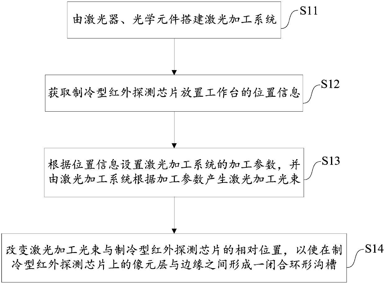
[0066] Embodiments of the present invention provide a method for laser processing chips, such as figure 1 As shown, the method includes:

[0067] S11. Build a laser processing system with lasers and optical components;

[0068] S12. Acquiring the position information of the workbench where the cooled infrared detection chip is placed;

[0069] S13. Set the processing parameters of the laser processing system according to the position information, and generate the laser processing beam according to the processing parameters by the laser processing system;

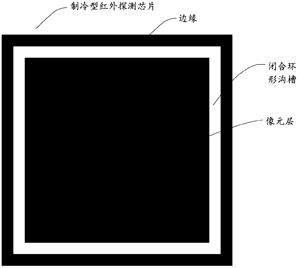
[0070] S14. Changing the relative position of the laser processing beam and the cooled infrared detection chip, so that a closed annular groove is formed between the pixel layer and the edge on the cooled infrared detection chip.

[0071] The method for laser processing chips provided by the embodiments of the present invention mainly uses laser processing systems to generate laser beams to prepare closed annular grooves o...

Embodiment 2

[0124] The difference between this embodiment and Embodiment 1 is that a single laser processing beam can not be used for laser cutting to obtain a groove bottom structure with high flatness. Therefore, the embodiment of the present invention provides a method for laser processing chips, such as Figure 6 As shown, the method includes:

[0125] S41. Build a laser processing system with lasers and optical components;

[0126] S42. Obtain the position information of the workbench where the cooling type infrared detection chip is placed;

[0127] S43. Set the processing parameters of the laser processing system according to the position information, and generate the laser processing beam according to the processing parameters by the laser processing system;

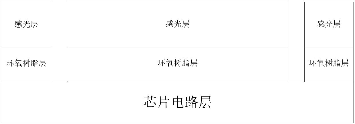
[0128] S44. Process the photosensitive layer of the cooled infrared detector chip with the laser processing beam with the first power to form two parallel grooves, and then process the cooled infrared detector chip between ...

Embodiment 3

[0159] The difference between this embodiment and the above-mentioned embodiment is that the narrower the width of the prepared groove, the better, and the depth just penetrates to the bottom readout chip circuit layer, and the two sides of the groove are steep, which is conducive to the release of stress; therefore, the embodiment of the present invention provides A method of laser processing chips, such as Figure 8 As shown, the method includes:

[0160] S51. Build a workbench with adjustable angle, and place the refrigerated infrared detection chip to be processed on the workbench;

[0161] S52, setting the adjustment and compensation process parameters of the workbench, and the laser parameters of the laser processing system built by the laser and optical components;

[0162] S53. Change the angle of the workbench at least once according to the laser parameters, adjust and compensate the process parameters, so that the laser processing system performs inclined processing...


PUM

PropertyMeasurementUnit
Wavelengthaaaaaaaaaa
Heightaaaaaaaaaa

Abstract

The invention provides a laser processing chip method and device. The laser processing chip method comprises the following steps that a laser device and an optical element is used for building a laserprocessing system; the processing deviation of the constructed laser processing system is detected; drawing parameters of the groove to be processed is obtained according to the processing deviationamount; and the laser processing system is used for processing the refrigeration type infrared detection chip according to the drawing parameters of the groove to be processed, so that a closed annular groove is formed between the pixel layer and the edge on the refrigeration type infrared detection chip. According to the laser processing chip method and device, the pixel utilization rate at the corner of the closed annular groove can be effectively improved, the influence on the width and the depth uniformity of the groove at the corner is reduced, and finally the effect of the laser groovingand the reliability of the chip are improved.

Description

technical field [0001] The invention relates to the technical field of laser micromachining, in particular to a method and device for laser machining chips. Background technique [0002] Infrared detectors have been well used in both civil and military applications, and the performance of cooled infrared detectors is particularly excellent. The infrared detection chip in the cooling type infrared detector is often in an environment with drastic temperature changes. In order to ensure its normal working performance, the infrared detection chip in the detector needs to be cooled with liquid nitrogen during the working state. The temperature at this time is about It is -200°C, but during non-working hours, the infrared detection chip is exposed to the atmospheric temperature. For example, the highest temperature in the desert can sometimes reach about 70°C, so the ambient temperature of the infrared detection chip is between -200°C and Constantly changing between 70°C. [000...

Claims


Application Information

Patent Timeline
IPC IPC(8): B23K26/364B23K26/064B23K26/70
CPCB23K26/0643B23K26/0648B23K26/064B23K26/364B23K26/702
Inventor 李纪东侯煜张喆李曼王然张紫辰
Owner 北京中科镭特电子有限公司
Why Eureka
Try Eureka