Magnetic structure and sot-mram based on artificial antiferromagnetic pinned layer

An artificial antiferromagnetic and magnetic structure technology, which is applied in the field of magnetic field controlled resistors, material selection, digital memory information, etc., can solve the problems of high write current density and limit the arrangement density of memory cell arrays, so as to improve the arrangement Density, fast write response speed, and reduced device volume

Active Publication Date: 2021-01-19
XI AN JIAOTONG UNIV
View PDF5 Cites 0 Cited by
  • Summary
  • Abstract
  • Description
  • Claims
  • Application Information

AI Technical Summary

Problems solved by technology

However, the write current density of this SOT-MRAM is still very high, which limits the arrangement density of the memory cell array.

Method used


Image

  • Magnetic structure and sot-mram based on artificial antiferromagnetic pinned layer
  • Magnetic structure and sot-mram based on artificial antiferromagnetic pinned layer
  • Magnetic structure and sot-mram based on artificial antiferromagnetic pinned layer

Examples


Embodiment Construction

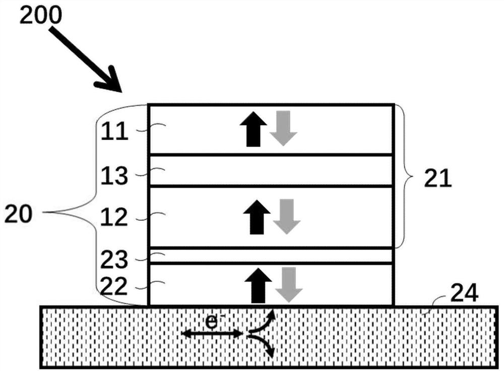
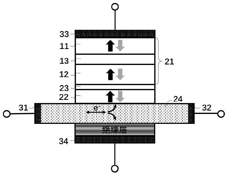
[0038] The technical solutions of the present invention will be described in detail below with reference to the accompanying drawings and embodiments. The following embodiments relate to a magnetic random access memory that enhances the antiferromagnetic coupling of artificial antiferromagnetic devices through electric field regulation, but does not constitute any basis for limiting the present invention.

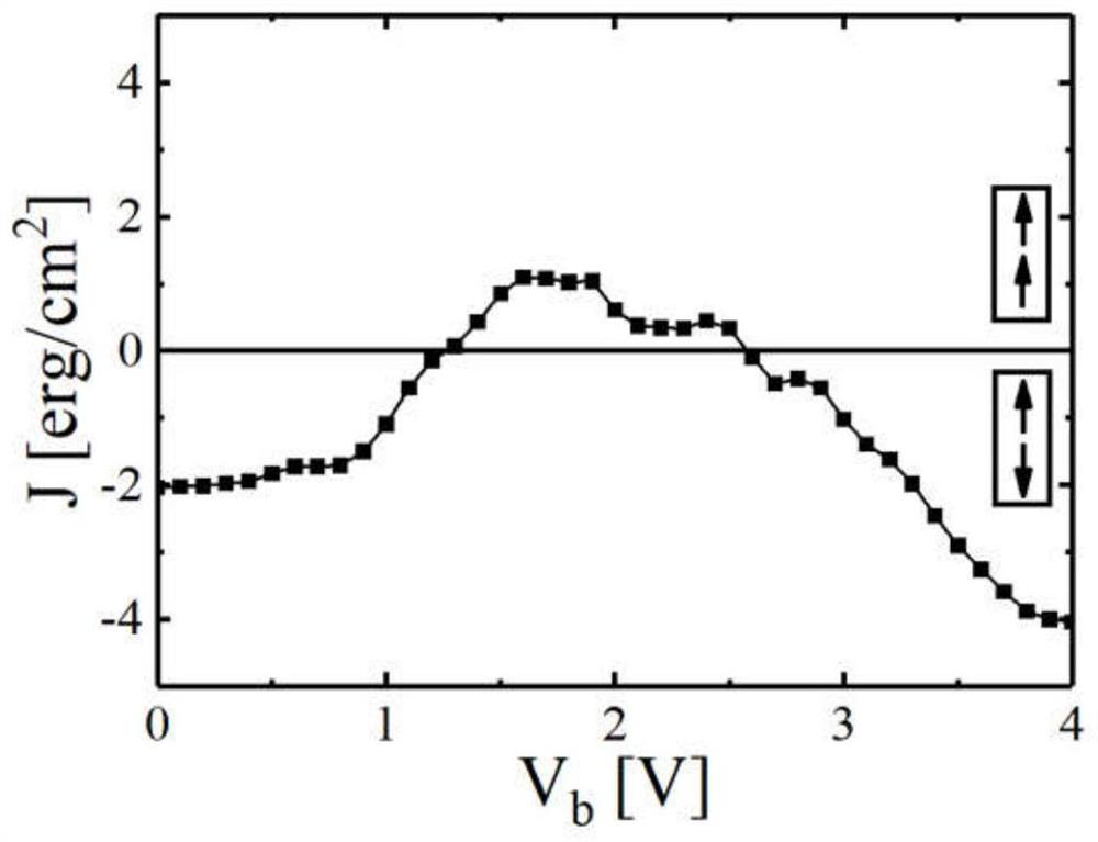
[0039] figure 1 is our research result, which shows the change of the antiferromagnetic coupling strength J when the artificial antiferromagnetic device is regulated by voltage. When the ferromagnetic layer is [Pt(0.88nm)|Co(0.70nm)] 2 , the degree of interface disorder is 0.5, and the thickness of Ru is 0.66nm, the artificial antiferromagnetic device has a relatively weak antiferromagnetic coupling in the initial state, and it can be transformed into a strong antiferromagnetic coupling when the applied electric field is increased to 4V coupling. It can be seen from the f...


PUM

PropertyMeasurementUnit
diameteraaaaaaaaaa

Abstract

The invention discloses a magnetic structure based on an artificial antiferromagnetic fixed layer and a spin-orbit torque-random magnetic memory (Spin-Orbit Torque Magnetic Random Access Memory, SOT-MRAM), which includes an artificial antiferromagnetic The magnetic tunnel junction of the pinned layer of the magnetic device and a spin-orbit moment material layer; the pinned layer based on the artificial antiferromagnetic device can be controlled by an electric field to achieve its antiferromagnetic coupling enhancement. The device can realize stable writing of data under the joint action of electric field and current, and has the advantages of simple structure, high density, low power consumption, fast speed, radiation resistance and non-volatility.

Description

technical field [0001] The present invention relates to circuits and devices with magnetic / ferromagnetic materials or structures and applications thereof, more specifically, to a fixed layer based on an artificial antiferromagnetic device regulated by an electric field and a device for data erasing and writing using spin-orbit moments Spin-Orbit Torque Magnetic Random Access Memory (SOT-MRAM). Background technique [0002] Magnetic Tunnel Junction (Magnetic Tunnel Junction, MTJ) is composed of two magnetic metal layers and an ultra-thin insulating layer sandwiched between them. If a bias voltage is applied between the two magnetic metal layers, since the insulating layer is very thin, electrons can pass through its potential barrier through the tunneling effect. Under a given bias voltage, the size of the tunneling current / tunneling resistance depends on the relative orientation of the magnetization in the two ferromagnetic layers (parallel or antiparallel, corresponding to...

Claims


Application Information

Patent Timeline
Patent Type & Authority Patents(China)
IPC IPC(8): H01L43/08H01L43/06H01L43/10G11C11/16
CPCG11C11/161H10N52/00H10N50/10H10N50/85
Inventor 闵泰周学松周雪王蕾
Owner XI AN JIAOTONG UNIV
Why Eureka
Try Eureka