Method and system for detection and fault positioning of SoC chip through laser simulation single particle irradiation

A single-particle irradiation, fault location technology, applied in electronic circuit testing, electrical measurement, measuring devices, etc., can solve problems such as unfavorable chip flip characteristics, large chip flip cross-section, large laser spot, etc., to prevent the impact of test results. , high coverage, rich experimental conditions and effects of methods

Active Publication Date: 2019-04-05
BEIJING MXTRONICS CORP +1
View PDF12 Cites 10 Cited by
  • Summary
  • Abstract
  • Description
  • Claims
  • Application Information

AI Technical Summary

Problems solved by technology

However, due to the large laser spot, it is easy to cause the problem of multi-bit flipping, which will make the flipping section of the chip too large, which is not conducive to truly reflecting the flipping characteristics of the chip; moreover, most of the lasers are pulsed lasers, and the laser frequency and the step distance of the mechanical translation stage need to be coordinated with each other. Otherwise, repeated irradiation or missed irradiation may occur

Method used


Image

  • Method and system for detection and fault positioning of SoC chip through laser simulation single particle irradiation
  • Method and system for detection and fault positioning of SoC chip through laser simulation single particle irradiation
  • Method and system for detection and fault positioning of SoC chip through laser simulation single particle irradiation

Examples


Embodiment Construction

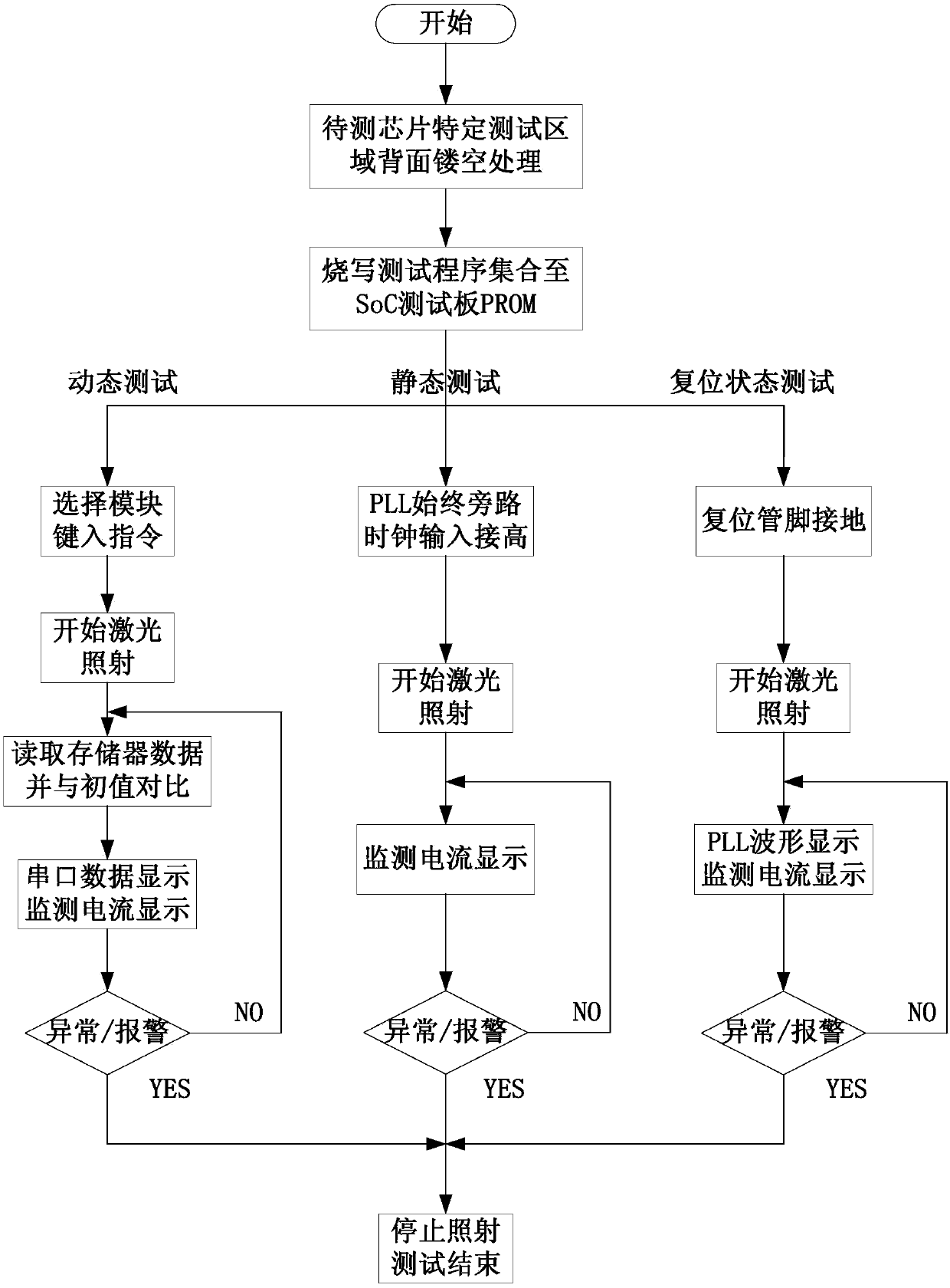
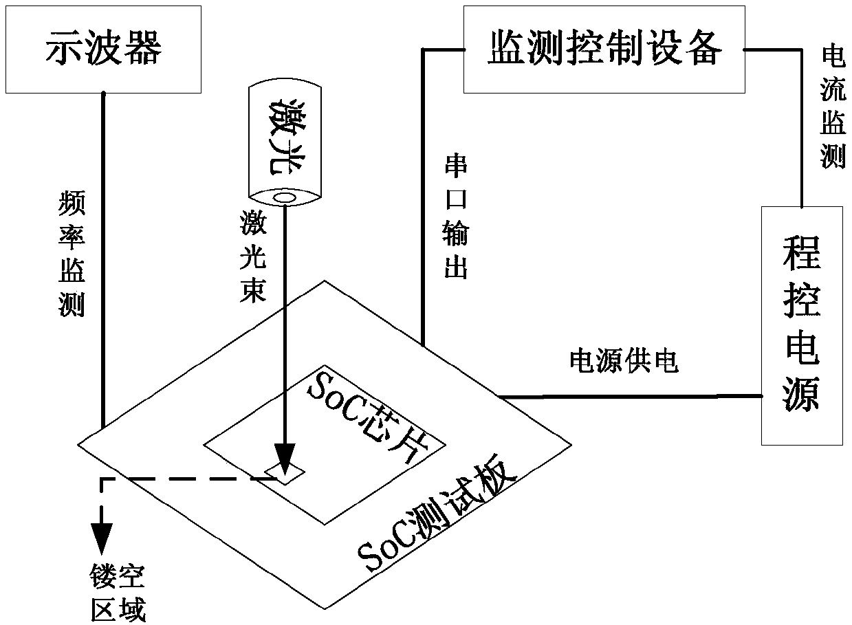
[0059] Such as figure 1 As shown, in view of the technical difficulties of laser simulation single event effect testing in the prior art, the present invention proposes a SoC chip laser simulation single event radiation detection and fault location method, including reset mode, static mode and dynamic mode three test modes, The specific steps for each mode are as follows:

[0060] 1. Steps in reset mode:

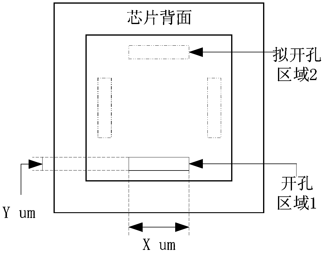
[0061] (1-1), the back side of the SoC chip area to be tested is opened to expose the chip substrate;

[0062] The maximum scanning speed of the selected laser is 100um / s. In order to reduce the impact of the laser on the non-test area due to the hole opening process error, the hole opening accuracy is preferably controlled within 100um. When the area to be tested affects die bonding, the area to be tested can be divided into multiple sub-areas, and multiple SOC chip tests are performed on each sub-area to obtain test results. Such as figure 1 As shown, when the area to ...


PUM


Abstract

The invention provides a method and system for detection and fault positioning of a SoC chip through laser simulation single particle irradiation. The method comprises the following steps of (1) performing hollowed-out processing on a test area of a to-be-tested chip; (2) if dynamic testing is carried out, selecting a function testing program of a certain module, starting function testing, and outputting a testing result; (3) if static testing is carried out, bypassing a PLL clock, stopping clock signal input, and detecting a circuit state through the current change; and (4) if reset state testing is carried out, connecting a reset pin to the ground, enabling the SOC chip to be continuously in a reset state through a reset circuit, and detecting the circuit state by observing the current change and a phase-locked loop frequency waveform. According to the method and system, the influence of larger laser spots on a non-test area is avoided, and the comprehensiveness and the accuracy of SOC chip testing are improved.

Description

technical field [0001] The invention relates to the field of single event effect test technology and methods, in particular to methods for testing and detecting devices such as SoC chips by irradiating laser simulated single event effects, finding problems and finding and locating faults. Background technique [0002] Spacecraft are exposed to high-energy particles such as galactic cosmic rays, solar cosmic rays, Earth radiation belt particles, and atmospheric neutrons in outer space. Single event effects are prone to occur when devices are irradiated by high-energy particles. With the continuous improvement of chip manufacturing technology and integration, the feature size of semiconductor devices continues to shrink, and integrated circuits are becoming more and more sensitive to space radiation effects. Carrying out the research and analysis of the single event effect of aerospace electronic devices is of great significance for improving the stability of spacecraft opera...

Claims


Application Information

Patent Timeline
Patent Type & Authority Applications(China)
IPC IPC(8): G01R31/28
CPCG01R31/2851
Inventor 尤利达陈雷于立新彭和平庄伟张世远
Owner BEIJING MXTRONICS CORP
Why Eureka
Try Eureka