
Double grating nanostructure composed of quadrangular double cone arrays and preparing method thereof

A nanostructure, four-corner biconical technology, applied in nanotechnology, nano-optics, nanotechnology, etc., can solve problems such as hindering the improvement of geometry and affecting the AR effect of pyramidal gratings, and achieve the effect of improving light sensitivity

Active Publication Date: 2019-04-05
THE CHINESE UNIV OF HONG KONG SHENZHEN
View PDF13 Cites 1 Cited by
  • Summary
  • Abstract
  • Description
  • Claims
  • Application Information

AI Technical Summary

Problems solved by technology

However, the anisotropic etching characteristic of silicon hinders further improvement of the geometry, thus affecting the AR effect of the pyramidal grating

Method used


Image

  • Double grating nanostructure composed of quadrangular double cone arrays and preparing method thereof
  • Double grating nanostructure composed of quadrangular double cone arrays and preparing method thereof
  • Double grating nanostructure composed of quadrangular double cone arrays and preparing method thereof

Examples


preparation example Construction

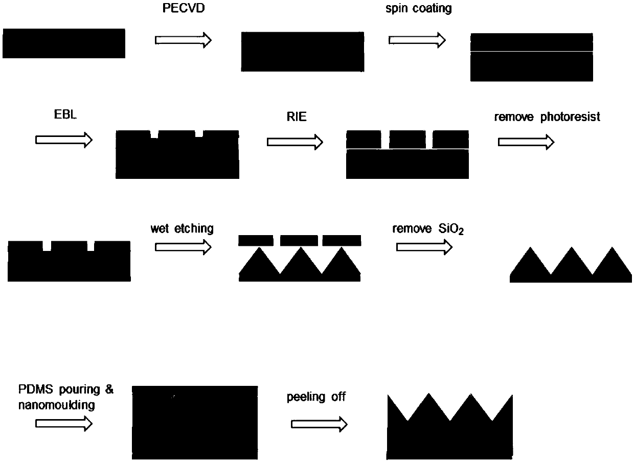
[0033] The embodiment of the present invention also provides a method for preparing a double-grating nanostructure composed of the above-mentioned quadrangular bipyramid array, which includes:

[0034] S1. abutting the installation surfaces of two porous silicon substrates that are mirror images of each other, so that the holes of the two porous silicon substrates correspond one by one to form a plurality of quadrangular biconical cavities;

[0035] S2. Fill polydimethylsiloxane in multiple cavities to form multiple grating nanostructure units;

[0036] S3. Peel off any one of the two porous silicon substrates to obtain a double grating nanostructure.

[0037] Further, in the actual operation process, in order to facilitate the operation, the way to fill polydimethylsiloxane in multiple cavities is to first drop polydimethylsiloxane on the mounting surface of one of the porous silicon substrates , and then covered with another porous silicon substrate, in the process of align...

Embodiment

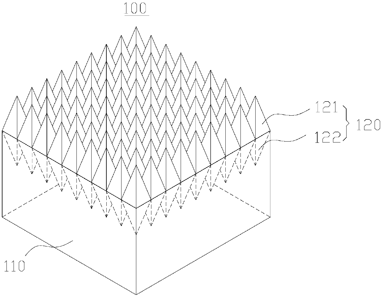
[0055] This embodiment provides a double grating nanostructure 100 composed of a quadrangular bipyramid array, the structure of which is as follows figure 1 As shown, it includes a porous silicon substrate 110 and a plurality of grating nanostructure units 120 .

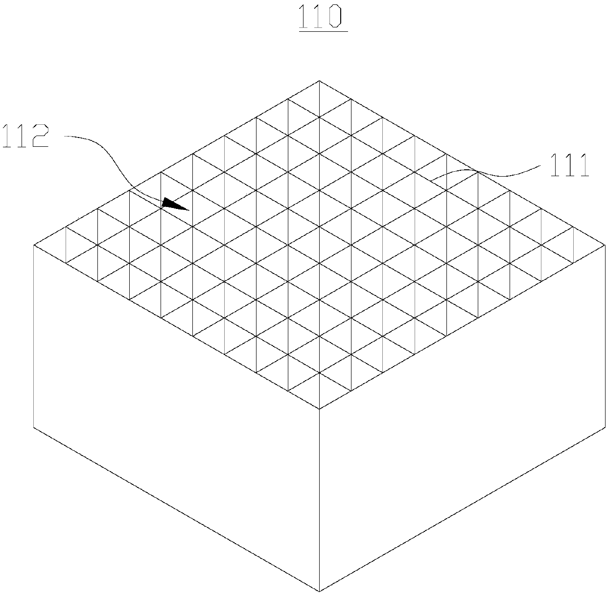
[0056] Wherein, the porous silicon substrate 110 includes a mounting surface 111, and a plurality of holes 112 for installing the grating nanostructure unit 120 are arrayed on the mounting surface 111. The shape of the holes 112 is an inverted quadrangular pyramid, and the apex of the quadrangular pyramid faces the porous silicon substrate. Inside, the bottom surface is located on the mounting surface 111 . The quadrangular pyramid-shaped hole 112 has a depth of 700 nm and a bottom surface of a square with a side length of 200 nm.

[0057] The material of the grating nanostructure unit 120 is polydimethylsiloxane. A plurality of grating nanostructure units 120 correspond to a plurality of holes 112, and each gratin...


PUM

PropertyMeasurementUnit
heightaaaaaaaaaa
thicknessaaaaaaaaaa

Abstract

The invention relates to a double grating nanostructure composed of quadrangular double cone arrays, and relates to the field of optical devices. The double grating nanostructure comprises a porous silicon substrate and a plurality of grating nanostructure units. Each grating nanostructure unit is in a quadrangular double-cone shape, wherein a half is buried in the porous silicon substrate, and the other half is exposed outside the porous silicon substrate. The grating nanostructure units in the quadrangular double-cone shapes can provide more gradual effective refractive index distribution between air and the device, and the light sensitivity, the light energy collection rate and the like of the device are further improved. A preparation method of the double grating nanostructure composedof the quadrangular double cone arrays is simple in operation, not high in requirement for equipment, and capable of being conveniently used for preparation of the double grating nanostructure composed of the above quadrangular double cone arrays.

Description

technical field [0001] The invention relates to the field of optical devices, in particular to a double-grating nanostructure composed of a quadrangular bipyramid array and a preparation method thereof. Background technique [0002] Today's light energy utilization and collection has entered a period of rapid development, in which more sensitive light collection (photodetectors) and more light energy collection (solar cells) are becoming more and more important. In order to achieve the above goals and reduce the loss of light due to reflection, many scientists focus on the wide-band anti-reflection (Antireflection, AR) performance of the surface of the instrument and the performance under the large angle of incidence (Angle of Incidence, AOI). For thin-film solar cells, These properties are even more important in various devices such as optical oscilloscopes and photodetectors. [0003] As a traditional way, half-wavelength AR coatings are widely used to reduce the reflecti...

Claims


Application Information

Patent Timeline
Patent Type & Authority Applications(China)
IPC IPC(8): G02B5/18G03F1/80G03F7/00B82Y20/00B82Y40/00
CPCB82Y20/00B82Y40/00G02B5/18G03F1/80G03F7/00
Inventor 张昭宇袁牧锋崔雨舟
Owner THE CHINESE UNIV OF HONG KONG SHENZHEN
Learn More