CMOS (complementary metal oxide semiconductor) image sensor and manufacturing method thereof

A technology of an image sensor and a production method, which is applied in the directions of image communication, radiation control device, television, etc., can solve the problems of increasing production cost and achieve the effect of enhancing light sensitivity

Inactive Publication Date: 2012-06-27
SHANGHAI HUAHONG GRACE SEMICON MFG CORP
View PDF3 Cites 5 Cited by
  • Summary
  • Abstract
  • Description
  • Claims
  • Application Information

AI Technical Summary

Problems solved by technology

However, its production cost increases more

Method used


Image

  • CMOS (complementary metal oxide semiconductor) image sensor and manufacturing method thereof
  • CMOS (complementary metal oxide semiconductor) image sensor and manufacturing method thereof
  • CMOS (complementary metal oxide semiconductor) image sensor and manufacturing method thereof

Examples


Embodiment 1

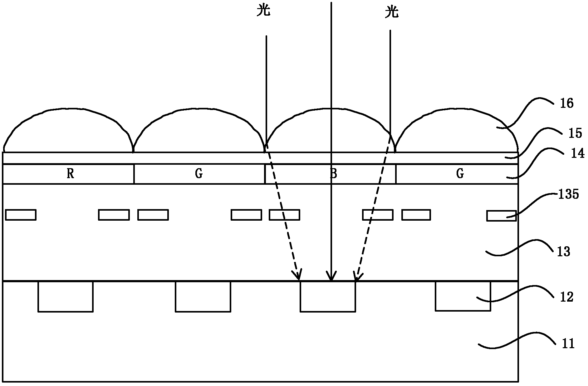
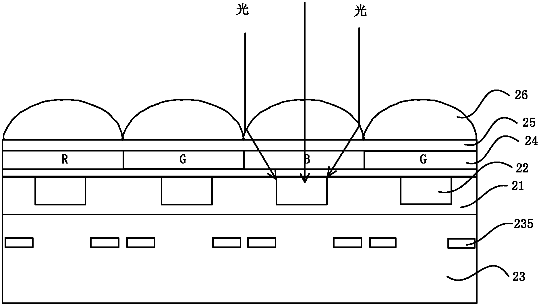
[0047] In order to avoid the situation mentioned in the background technology that the light collected by the microlens is blocked by the metal connection layer and cannot fully reach the photodiode, or other situations that affect the light sensitivity occur, the embodiments of the present invention are based on the original microlens and the photoelectric A second microlens is added between the diodes. The second microlens further adjusts the light collected by the original microlens. On the one hand, it prevents the light from being blocked by the metal connection layer and cannot reach the photodiode. On the other hand, it can also prevent the light from being blocked by the original microlens The situation where the lens is over-converged so that some areas of the photodiode receive excessive light, and some areas have no light incident.

[0048] The structure of a CMOS image sensor (CIS) and its fabrication method according to a first embodiment of the present invention w...

Embodiment 2

[0062] The structure of the product provided by this embodiment is the same as that of Embodiment 1, and the only difference lies in the manufacturing method of the microlens. The manufacturing method and advantages of the microlens used in this embodiment will be mainly introduced below.

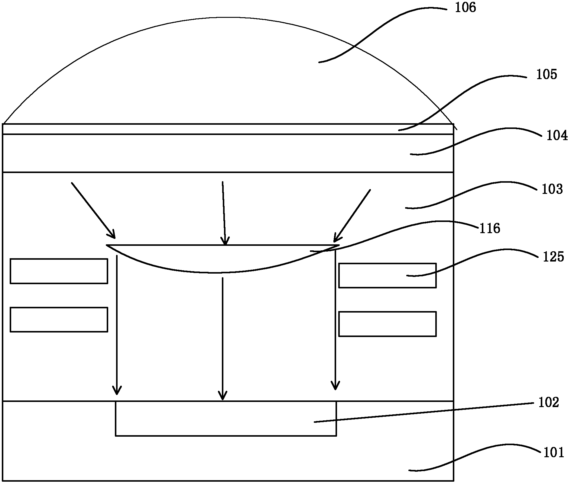
[0063] Figure 4 to Figure 7 is a cross-sectional view showing a method of manufacturing a microlens or a microlens array (MLA). refer to Figure 4 , depositing a dielectric layer 303 , where the dielectric layer may be part of the interlayer insulating layer 103 in Embodiment 1. Next, a barrier layer 305 is formed over the entire surface of the top of the layer 303 . The barrier layer can be made of silicon nitride film (Si 3 N 4 )form.

[0064] Then, a PR pattern 307 for forming a microlens pattern is formed. PR (photoresist) is coated over the entire surface of the top of the barrier layer 305 . Portions of the top PR are selectively removed by performing an exposure process usin...


PUM


Abstract

The invention provides a CMOS (complementary metal oxide semiconductor) image sensor and a manufacturing method thereof. The CMOS image sensor comprises a photodiode, a first micro lens and a metal connection layer, wherein the first micro lens is used for focusing the incident light to a position where the photodiode is arranged, and the metal connection layer is positioned between the photodiode and the first micro lens and exposes at least part of the photodiode. The CMOS image sensor further comprises a second micro lens which is arranged between the first micro lens and the photodiode and positioned outside the metal connection layer. Since the second micro lens is additionally arranged between the first micro lens and the photodiode, luminous sensitivity of the CMOS image sensor is improved with manufacturing cost barely increased.

Description

technical field [0001] The present invention relates to CMOS image sensor devices and methods of forming the same. Background technique [0002] An image sensor is a device that converts one-dimensional or two-dimensional optical information into electrical signals. Image sensors can be classified into two types: image pickup tubes and solid image pickup devices. The camera tube is widely used in related fields of measurement, control, and identification compatible with image processing technology centered on television. Various imaging tube-based application technologies have been developed. [0003] Image sensors can be further classified into two different types: Complementary Metal Oxide Semiconductor (CMOS) type and Charge Coupled Device (CCD) type. Compared with CCD image sensors, CMOS image sensors (CMOS image sensors may be referred to as CIS) have more convenient driving modes and can realize various scan types. Also, the integration of signal processing circuit...

Claims


Application Information

Patent Timeline
Patent Type & Authority Applications(China)
IPC IPC(8): H01L27/146H04N5/374
Inventor 巨晓华张克云孔蔚然
Owner SHANGHAI HUAHONG GRACE SEMICON MFG CORP
Why Eureka
Try Eureka