Novel n type semi-insulating GaAs ohmic contact electrode material and method for preparing novel n type semi-insulating GaAs ohmic contact electrode material

An ohmic contact electrode, semi-insulating technology, applied in the direction of final product manufacturing, circuits, electrical components, etc., to achieve the effect of low cost, good economic benefits, and short process

Active Publication Date: 2014-05-14
HUAIYIN TEACHERS COLLEGE
View PDF7 Cites 4 Cited by
  • Summary
  • Abstract
  • Description
  • Claims
  • Application Information

AI Technical Summary

Problems solved by technology

In the early days of the existing technology, n-GaAs used AuGe eutectic alloy to make electrodes. The process was to anneal at high temperature after vacuum evaporation to achieve eutecticization. It is uneven, and what’s more, the electrode can fall off; in order to solve this problem, researchers in the industry added Ni to the eutectic process to prevent Au from pilling; in the subsequent process improvement, tungsten nitride (WN) was added As an anti-diffusion layer, Au is finally evaporated to form an ohmic contact electrode
It can be seen that the current GaAs ohmic contact electrode material is not only complicated in manufacturing process, but also expensive

Method used


Image

  • Novel n type semi-insulating GaAs ohmic contact electrode material and method for preparing novel n type semi-insulating GaAs ohmic contact electrode material
  • Novel n type semi-insulating GaAs ohmic contact electrode material and method for preparing novel n type semi-insulating GaAs ohmic contact electrode material
  • Novel n type semi-insulating GaAs ohmic contact electrode material and method for preparing novel n type semi-insulating GaAs ohmic contact electrode material

Examples


Embodiment Construction

[0021] According to technical solution of the present invention, enumerate embodiment as follows:

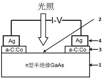
[0022] First, a Co-doped non-carbon crystal film was plated on the substrate by pulsed laser deposition. The resistivity of the substrate is about 5×10 8 Ω.cm undoped n-type semi-insulating GaAs material. Graphite with a purity of 99.99% and metal Co with a purity of 99.9% are used as the target source, and the metal Co sheet is attached to the graphite target, and the pulse laser deposition coating is performed on the two electrode areas set on the n-type semi-insulating GaAs substrate. During the coating process, uniform doping is achieved by the rotation of the target and the substrate, and the Co doping amount is about 10 at% (atomic percentage). Laser energy 450 mJ / pulse, cavity vacuum 5×10 -5 Pa, the substrate temperature is controlled at about 450°C, and the distance between the target and the substrate is 5.5cm. The non-carbon crystal film is plated with a thickn...


PUM

PropertyMeasurementUnit
electrical resistivityaaaaaaaaaa
lattice constantaaaaaaaaaa
thicknessaaaaaaaaaa

Abstract

The invention provides a novel n type semi-insulating GaAs ohmic contact electrode material and a method for preparing the novel n type semi-insulating GaAs ohmic contact electrode material. According to the method for preparing the novel n type semi-insulating GaAs ohmic contact electrode material, an undoped n type semi-insulating GaAs substrate is adopted to serve as an electrode bottom layer, two electrode areas on the substrate are plated with Co-doped amorphous carbon (a-C) films with the pulsed laser deposition method, the amorphous carbon films are plated with Ag with the vacuum heat evaporation method, and then the novel n type semi-insulating GaAs ohmic contact electrode material is obtained. According to various data detection results, the novel n type semi-insulating GaAs ohmic contact electrode material has the advantages that the I-V curve of an electrode has good linear relation and symmetric relation, all performance indexes meet requirements of stable contact electrodes, the luminous sensitivity is high, and the material can be successfully applied to devices relevant to n type semi-insulating GaAs; compared with a preparing technology in the prior art, the method for preparing the novel n type semi-insulating GaAs ohmic contact electrode material has the advantages that the processes are simple, cost is low, and the economic benefit is good.

Description

technical field [0001] The invention relates to semiconductor technology in the field of optoelectronics, in particular to a novel n-type semi-insulating GaAs ohmic contact electrode material and a preparation method thereof. Background technique [0002] Gallium arsenide (GaAs) is a III-V compound semiconductor with a zinc blende crystal structure. The lattice constant is 5.65×10 -10 m, the melting point is 1237°C, and the band gap is 1.42 electron volts. It can be made into a semi-insulating high-resistance material whose resistivity is more than 3 orders of magnitude higher than that of silicon and germanium, and is used in photoconductive switches, integrated circuit substrates, infrared detectors, gamma photon detectors, etc.; because its electron mobility is higher than that of silicon It is 5 to 6 times larger and has important applications in microwave devices and high-speed digital circuits; semiconductor devices made of GaAs have the advantages of high frequenc...

Claims


Application Information

Patent Timeline
Patent Type & Authority Applications(China)
IPC IPC(8): H01L31/0224H01L31/18
CPCH01L31/022425H01L31/18Y02P70/50
Inventor 翟章印胡小飞陈贵宾
Owner HUAIYIN TEACHERS COLLEGE
Why Eureka
Try Eureka