Automatic production method of PCB

A PCB board and production method technology, applied in the field of PCB board automation production, can solve the problems of low PCB board production efficiency, PCB board damage, low degree of automation, etc., and achieve the effects of ensuring production balance, reducing production costs, and excellent quality.

Inactive Publication Date: 2019-04-05
刘夏冰
View PDF5 Cites 15 Cited by
  • Summary
  • Abstract
  • Description
  • Claims
  • Application Information

AI Technical Summary

Problems solved by technology

[0004] The object of the present invention is to provide a kind of PCB board automatic production method, in order to overcome above-mentioned PCB board production method in actual application process, automation degree is low, needs a large amount of manual participation in most process steps, and whole PCB board production efficiency is low, and In the process of production, manual operation is likely to cause technical problems of PCB board damage

Method used


Image

  • Automatic production method of PCB
  • Automatic production method of PCB
  • Automatic production method of PCB

Examples


Embodiment Construction

[0037] The technical solutions of the present invention will be clearly and completely described below in conjunction with the embodiments. Apparently, the described embodiments are only some of the embodiments of the present invention, not all of them. Based on the embodiments of the present invention, all other embodiments obtained by persons of ordinary skill in the art without creative efforts fall within the protection scope of the present invention.

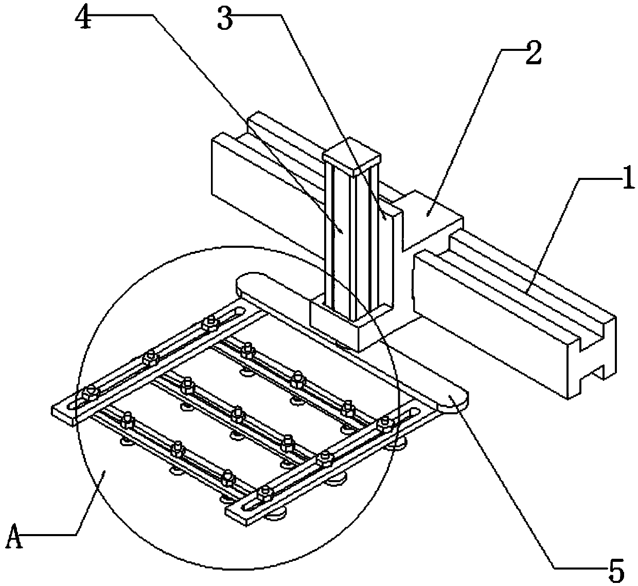
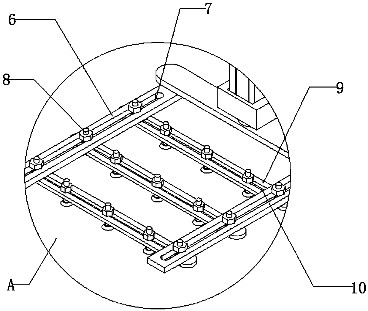
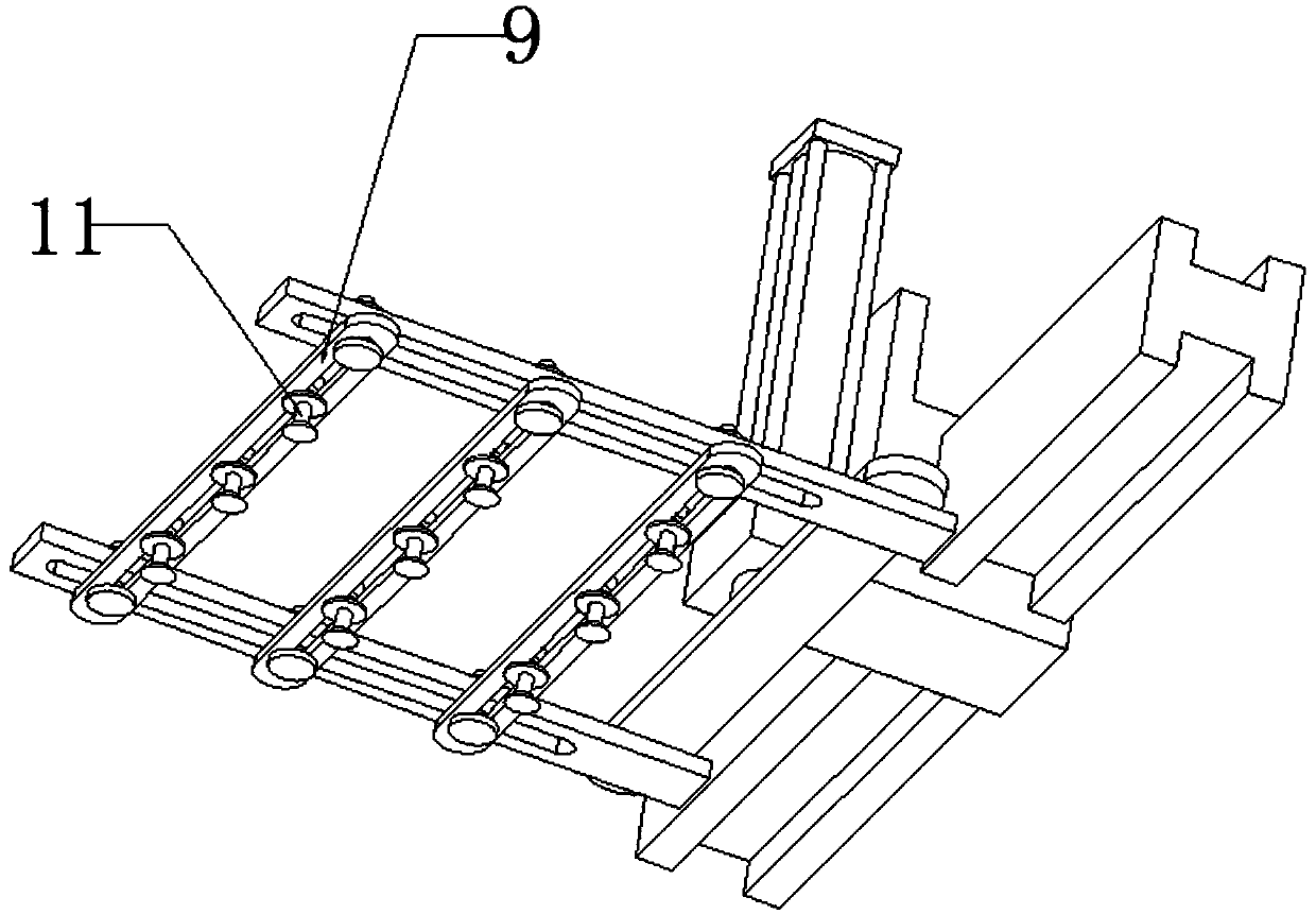
[0038] see Figure 1-3 As shown, a PCB board automatic production method, including material cutting - inner layer dry film - inner and outer layer intermediate inspection - browning process - inner laminate - drilling - sinking copper and board electricity - outer layer dry film - pattern electroplating - Whole board electric gold - outer layer etching - wet green oil - white characters - gold-plated fingers - tin spraying process - immersion gold process - shape processing steps, the specific steps are as follows:

[003...


PUM


Abstract

The invention discloses an automatic production method of a PCB. The automatic production method comprises the steps of material cutting, film drying at an inner layer, browning, inner-layer board lamination, copper deposition, board electroplating, film drying at an outer layer, gold electroplating, green oil wetting, goldfinger plating, tin spraying and gold deposition. In the step of material opening, a large material is cut to various fine materials by an automatic cutting machine according to specifications, a tip end of a round board is grinded by a round angle grinding machine, the board is placed in an oven for heating after the board is washed and dried by a board washing machine, the board is taken out after cooling and then is labeled as a mark; and in the step of film drying atthe inner layer, the board is placed in a chemical cleaning machine by a carrying device, and the cleaning is completed sequentially by washing, micro etching, high-pressure washing, cycle washing, water suction, strong wind blowing and hot-air secondary drying. The automatic production method is high in automation, the whole PCB production efficiency is high, and the damage to the PCB is low during the production process.

Description

technical field [0001] The invention relates to the field of automatic production of PCB boards, in particular to a method for automatic production of PCB boards. Background technique [0002] PCB board is also called printed circuit board, printed circuit board, referred to as printed board, with insulating board as the base material, cut to a certain size, with at least one conductive pattern attached to it, and holes (such as component holes, fastening holes) , metallized holes, etc.), used to replace the chassis of the previous device electronic components, and realize the interconnection between electronic components, because this board is made by electronic printing, it is called "printed" circuit board ; It is not accurate to call "printed circuit board" as "printed circuit" because there are no "printed components" but only wiring on the printed board. [0003] In the actual application process of the existing automatic production method of PCB board, the degree of ...

Claims


Application Information

Patent Timeline
Patent Type & Authority Applications(China)
IPC IPC(8): H05K3/00
CPCH05K3/00H05K2203/1545
Inventor 刘夏冰
Owner 刘夏冰
Why Eureka
Try Eureka