
Manufacturing method of OLED touch display screen

A technology of touch display screen and production method, which is applied in the direction of semiconductor/solid-state device manufacturing, electrical components, electric solid-state devices, etc., which can solve the problems of unfavorable flexible touch display screens such as thinning, bareness, and reduced electrical performance, and achieve improved The effect of equipment production capacity, avoiding functional failure, and simplifying production process

Active Publication Date: 2019-04-12
WUHAN CHINA STAR OPTOELECTRONICS SEMICON DISPLAY TECH CO LTD
View PDF5 Cites 6 Cited by
  • Summary
  • Abstract
  • Description
  • Claims
  • Application Information

AI Technical Summary

Problems solved by technology

[0004] With the rapid development of flexible display OLED technology, it is required that the matching touch screen also needs to be flexible and foldable. The traditional touch screen needs to be manufactured separately, and then bonded to the upper surface of the OLED with optical transparent glue to form a complete touch screen. The control display module increases the bonding process and also increases the overall thickness, which is not conducive to the overall thinning and thinning of the flexible touch display.
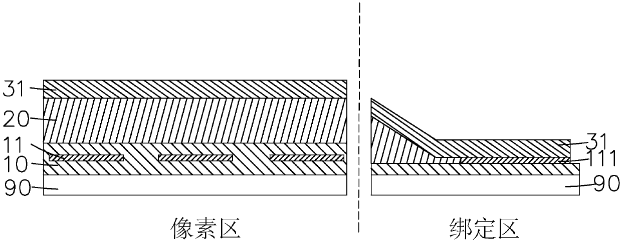
[0005] In the technical development of the existing external OLED touch display, the touch sensor is generally fabricated on the OLED layer. The specific process is as follows: firstly, the TFT layer including the substrate is fabricated, and the source and drain electrodes in the TFT layer The (SD) layer includes touch leads and binding pads for the touch part located in the binding area, then an OLED layer is made on the TFT layer, and finally a touch layer is made on the OLED layer; wherein the touch layer includes The first insulating layer, the bridge point layer, the second insulating layer, the electrode line layer and the protective layer are arranged in order from bottom to top, wherein the bridge point layer includes a plurality of metal bridges in the pixel area, and the electrode line layer includes a touch Drive electrodes, touch sensing electrodes and touch connection lines, the touch drive electrodes or touch sensing electrodes are connected to the metal bridge through the first contact holes penetrating through the second insulating layer, and the touch connection lines pass through The second contact holes of the first insulating layer and the second insulating layer are connected to the touch wires in the bonding area. Then, when performing the etching process, since the pixel area and the metal bonding area need to be etched at different depths, the prior art Generally, two photomasks are used to respectively etch the first insulating layer and the second insulating layer in the touch layer to form via holes with different depths in the via holes at both ends of the metal bridge and the metal bonding area. The manufacturing process of the SD layer requires at least 5 photomask processes, but after each photomask process is completed, the part of the SD layer used for the touch lead and the bonding pad will be etched and eroded, and then exposed, resulting in the surface of the SD layer Damaged or oxidized, reduced electrical performance or even failure
[0006] In addition, due to the water-phobic nature of OLED, the touch layer on the OLED layer should avoid too much contact with the wet etching process, while the conventional etching process in touch technology mainly uses a wet process process, although the dry process can avoid Wet contact, but it will also bring some other technical problems, especially when making the touch layer on the flexible OLED, for the protection of the structure, the pre-protection effect of the process needs to be considered

Method used


Image

  • Manufacturing method of OLED touch display screen
  • Manufacturing method of OLED touch display screen
  • Manufacturing method of OLED touch display screen

Examples


Embodiment Construction

[0039] In order to further illustrate the technical means adopted by the present invention and its effects, the following describes in detail in conjunction with preferred embodiments of the present invention and accompanying drawings.

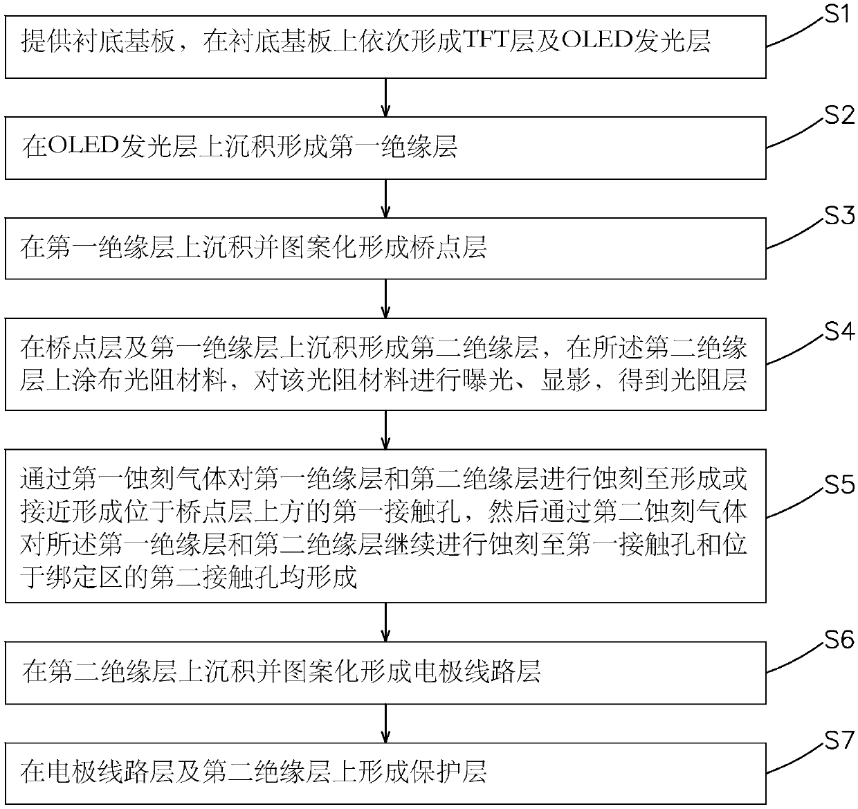
[0040] see figure 1 , the present invention provides a method for manufacturing an OLED touch display, the OLED touch display includes a pixel area located in the middle and a binding area located outside the pixel area, the method includes the following steps:

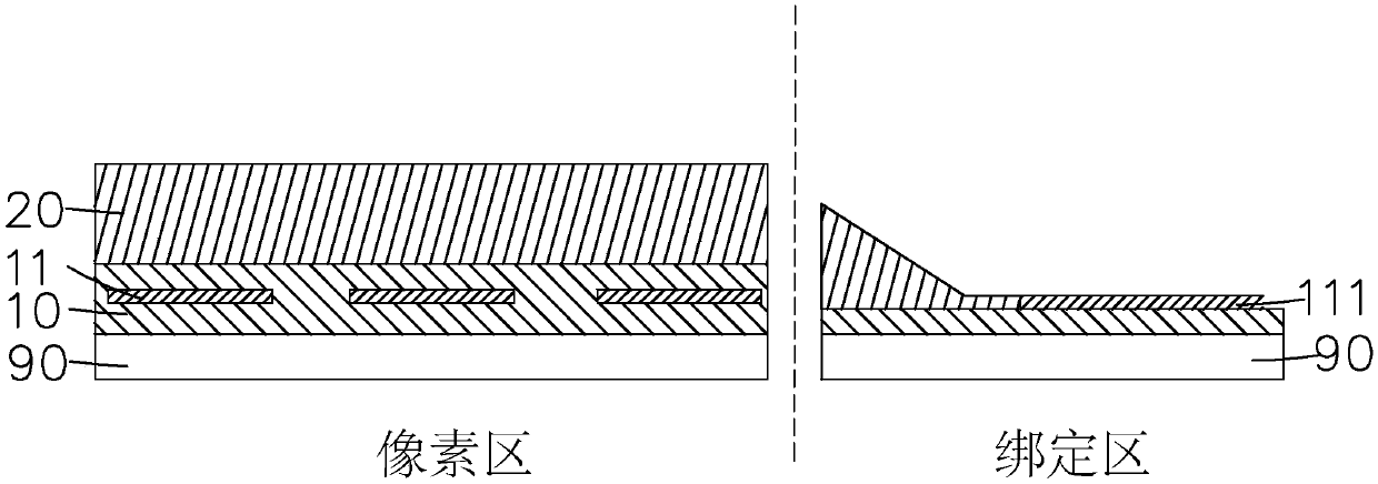
[0041] Step S1, such as figure 2 As shown, a base substrate 90 is provided, on which a TFT layer 10 and an OLED light emitting layer 20 are sequentially formed.

[0042] Specifically, in the step S1, the TFT layer 10 includes a buffer layer, an active layer, a gate insulating layer, a gate electrode layer, an interlayer insulating layer, a source-drain electrode layer 11 and a planarization layer, wherein the source The drain electrode layer 11 includes a touch wire 111 and a bonding...


PUM


Abstract

The invention provides a manufacturing method of an OLED touch display screen. A TFT layer, an OLED layer and a touch control layer are formed on a substrate in sequence. Compared with the prior art,when the touch control layer is manufactured, a first insulating layer is not etched before the first insulating layer is deposited and formed, and after a bridge point layer is deposited and formed;instead, the first insulating layer and a second insulating layer are subjected to dry etching synchronously by two kinds of etching gas in a matched mode after the second insulating layer is deposited and formed, so that the same-process manufacturing of contact holes of two different depths in the touch control layer can be realized, erosion of a wet etching process to the OLED is effectively lowered, the production process is simplified, and the production capacity of the device is improved; and meanwhile, a pre-protection effect on a touch lead and a binding pad in a source drain electrodelayer can be achieved, so that function invalidation caused by over-etching or oxidation is avoided.

Description

technical field [0001] The invention relates to the technical field of touch display, in particular to a method for manufacturing an OLED touch display. Background technique [0002] In flat panel display technology, Organic Light-Emitting Diode (OLED) display has many advantages such as thinness, active light emission, fast response speed, large viewing angle, wide color gamut, high brightness and low power consumption, etc., and has gradually become the successor. The third generation display technology after liquid crystal display. Compared with liquid crystal displays (Liquid crystal displays, LCD), OLED has the advantages of saving power, being thinner, and having a wider viewing angle, which is incomparable to LCD. At present, people have higher and higher requirements for the fineness of the display, that is, the resolution, but the production of high-quality, high-resolution OLED displays still faces many challenges. [0003] Currently, commonly used touch technolo...

Claims


Application Information

Patent Timeline
Patent Type & Authority Applications(China)
IPC IPC(8): H01L27/32H01L21/311
CPCH01L21/31116H01L21/31144H10K59/40H10K59/131
Inventor 冯校亮
Owner WUHAN CHINA STAR OPTOELECTRONICS SEMICON DISPLAY TECH CO LTD
Learn More