High-power quasi-continuous semiconductor laser chip

A quasi-continuous, semi-conductor technology, applied in the structural field of high-power quasi-continuous semiconductor laser chips, can solve the problems of large far-field slow-axis divergence angle, large threshold current, and poor optical mode characteristics, so as to improve device performance and reduce threshold current, low cost effect

Pending Publication Date: 2019-04-12
XIAN LIXIN PHOTOELECTRIC SCI & TECH
View PDF0 Cites 0 Cited by
  • Summary
  • Abstract
  • Description
  • Claims
  • Application Information

AI Technical Summary

Problems solved by technology

[0006] In order to solve the problems of large threshold current, poor optical mode characteristics and large divergence angle of the far-field slow axis in existing high-power quasi-continuous semiconductor laser chips, the present invention proposes an improved high-power quasi-continuous semiconductor laser chip

Method used


Image

  • High-power quasi-continuous semiconductor laser chip
  • High-power quasi-continuous semiconductor laser chip
  • High-power quasi-continuous semiconductor laser chip

Examples


Embodiment Construction

[0025] The present invention will be described in detail below in conjunction with the accompanying drawings and embodiments.

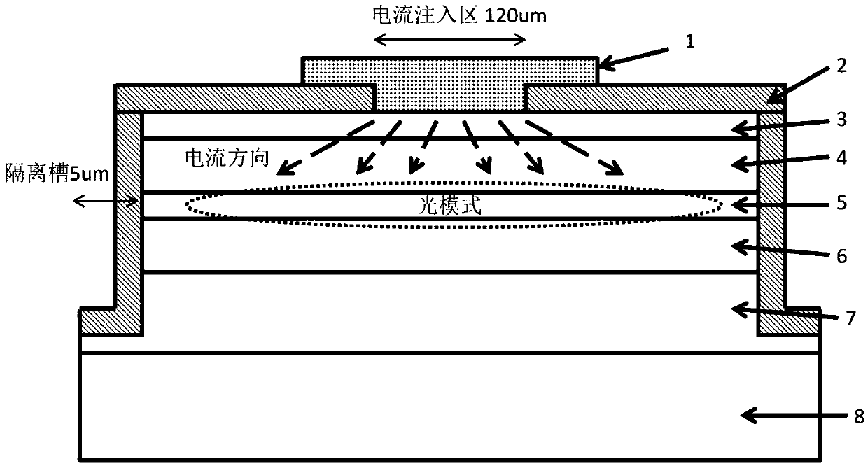
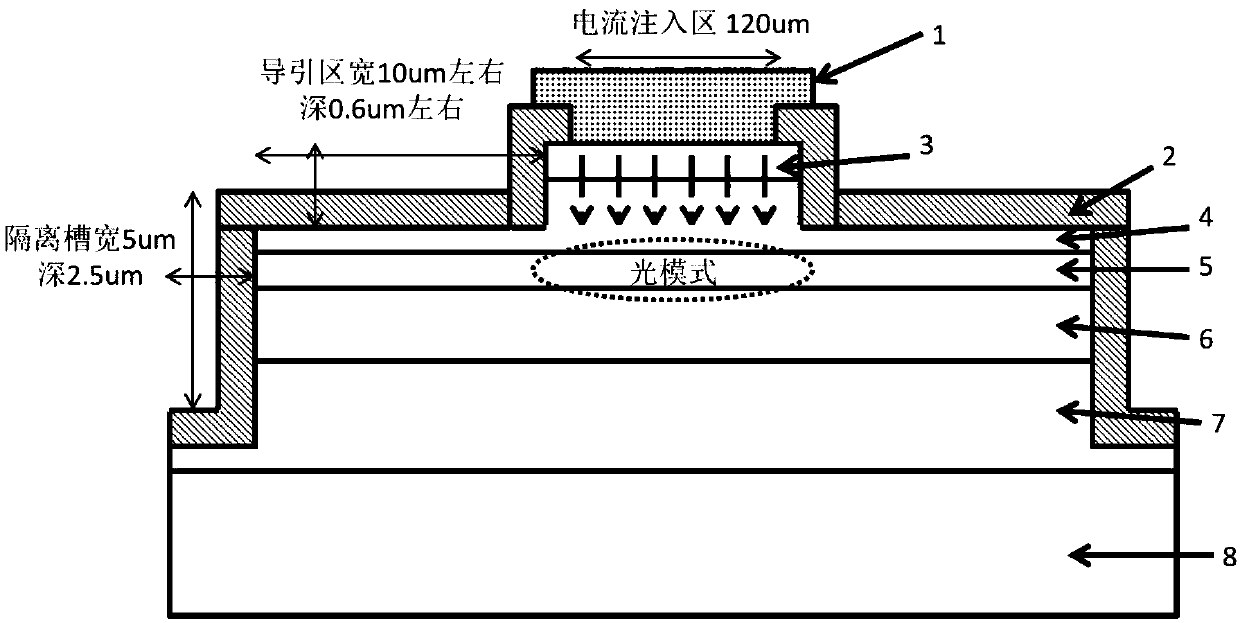
[0026] Such as figure 2 As shown, the present invention is based on a conventional semiconductor laser, including a substrate, an N-type buffer layer, an N-type confinement layer, a waveguide layer, a P-type confinement layer, a P-type contact layer and a metal electrode arranged sequentially from bottom to top. Isolation grooves are etched on the side (at least to the N-type buffer layer), and an insulating layer is provided on the surface of the device around the metal electrode and the isolation grooves on both sides. The present invention adds trench designs on both sides of the current injection region to limit the lateral diffusion of current and reduce the threshold current of the device. At the same time, due to the low refractive index of the insulating layer (about 1.5), a three-layer lateral refractive index is formed. Decreasing steps (w...


PUM


Abstract

The invention provides a high-power quasi-continuous semiconductor laser chip. A P-type limiting layer of the high-power quasi-continuous semiconductor laser chip is in a step shape, wherein the stepupper layer is limited to the middle region of the step foundation; a P type contact layer is limited to the surface of the step upper layer; an insulating layer correspondingly forms a bending shapeon the surface of a device, and sequentially covers 1) a region, not covered with a metal electrode, of the surface of the P type contact layer; 2) the side surface of the P type contact layer and theside surface o the stage upper layer; and 3) the surface of the step foundation. The high-power quasi-continuous semiconductor laser chip is simple in structure, and capable of effectively lowering the threshold current and the far-field divergence angle of the device, improving the performance of the device, and ensuring that the reliability is not affected, so that the chip meets the occasionswith higher requirements.

Description

technical field [0001] The invention relates to a structure of a high-power quasi-continuous semiconductor laser chip. Background technique [0002] High-power semiconductor lasers and their pumped solid-state lasers (Nd:YAG) have the advantages of high output optical power, high electro-optic conversion efficiency, high reliability, and compact structure, and are widely used in advanced manufacturing, medical beauty, aerospace, and entertainment displays. , security protection and other fields. As the requirements for the use of solid-state lasers become higher and higher, higher requirements are put forward for semiconductor lasers in terms of output power, electro-optical conversion efficiency, spectral width, beam quality, and reliability. [0003] For example, when a high-power quasi-continuous semiconductor laser is used as a pump source for a solid-state laser, in addition to the output power requirements, it also has requirements for the fast-axis divergence angle a...

Claims


Application Information

Patent Timeline
IPC IPC(8): H01S5/32H01S5/323
CPCH01S5/32H01S5/32316
Inventor 李青民孙丞仇伯仓李波
Owner XIAN LIXIN PHOTOELECTRIC SCI & TECH
Why Eureka
Try Eureka