Transceiver circuit for wireless charging and wireless charging system

A technology for transmitting and receiving circuits and wireless charging, which is applied in the direction of circuit devices and electrical components, can solve the problems of high energy consumption of equipment, energy conversion rate of less than 50%, energy loss, etc., and achieve the effect of improving conversion efficiency and solving low conversion efficiency

Inactive Publication Date: 2019-04-12
XIAN CREATION KEJI CO LTD
View PDF0 Cites 0 Cited by
  • Summary
  • Abstract
  • Description
  • Claims
  • Application Information

AI Technical Summary

Problems solved by technology

[0003] At present, the core issue that limits the large-scale application of wireless charging lies in the efficiency of power conversion, because in the process of wireless charging, the rectification of AC to DC and the inversion of DC to AC are required, as well as the need for transmission through electromagnetic waves. These processes will inevitably cause energy loss, especially to achieve long-distance high-power wireless magnetoelectric conversion, so the energy consumption of the equipment is relatively high
As the distance and power of wireless charging equipment increase, the consumption of useless work will also increase; at present, the energy conversion rate is less than 50% for a transmission distance greater than 50cm;

Method used


Image

  • Transceiver circuit for wireless charging and wireless charging system
  • Transceiver circuit for wireless charging and wireless charging system
  • Transceiver circuit for wireless charging and wireless charging system

Examples


Embodiment 1

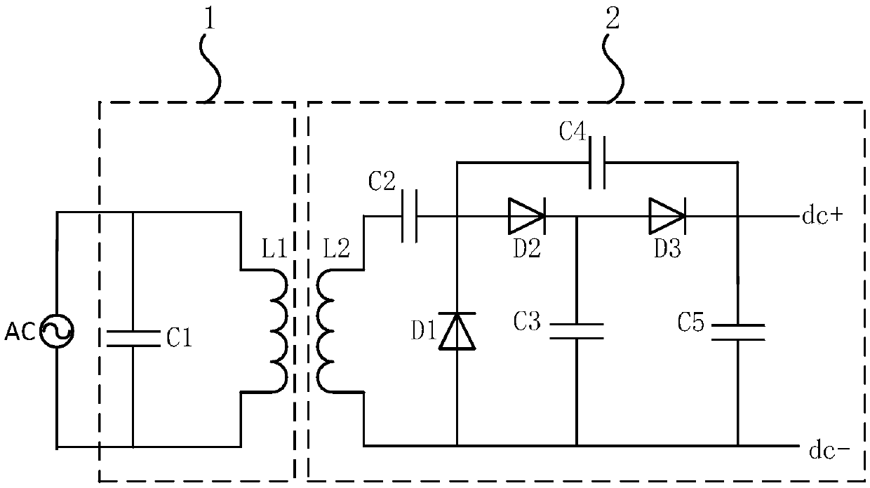
[0027] See figure 1 , figure 1 It is a schematic diagram of a transceiver circuit for wireless charging provided by an embodiment of the present invention. It includes: a transmitting circuit 1 and a receiving circuit 2; wherein, the transmitting circuit 1 includes: a first capacitor C1 and a transmitting coil L1; the receiving circuit 2 includes: a receiving coil L2, a second capacitor C2, a third capacitor C3, a first Four capacitors C4, fifth capacitor C5, first diode D1, second diode D2, third diode D3;

[0028] The upper plate and the lower plate of the first capacitor C1 are respectively electrically connected to the two ends of the transmitting coil L1, and the transmitting coil L1 is electrically coupled to the receiving coil L2; the first end of the receiving coil L2 is electrically connected to The upper plate of the second capacitor C2, the second end of the receiving coil L2 are respectively electrically connected to the anode of the first diode D1, the lower pla...

Embodiment 2

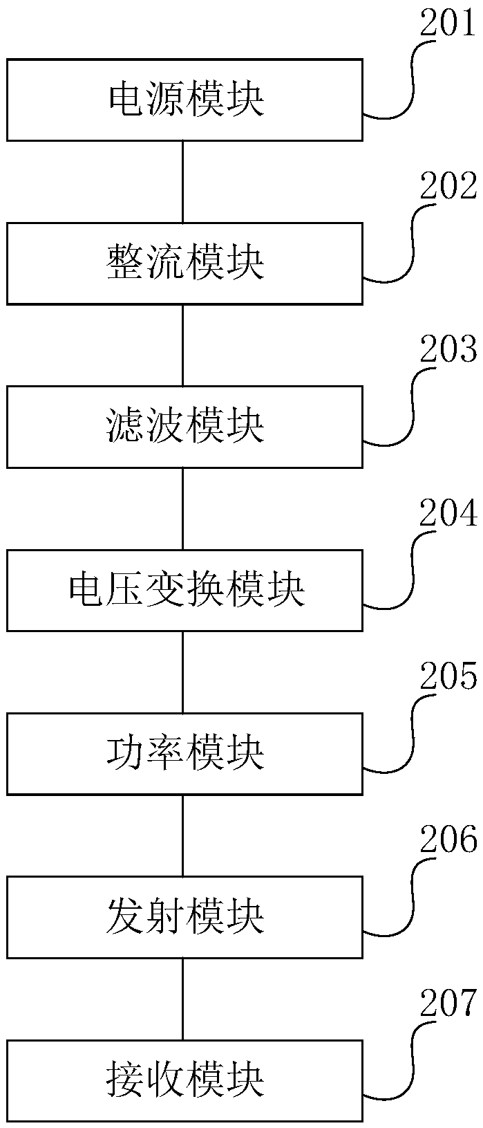
[0036] On the basis of Embodiment 1, this embodiment provides a wireless charging system, please refer to figure 2 , figure 2 It is a schematic diagram of a wireless charging system provided by an embodiment of the present invention.

[0037] The wireless charging system includes: a power supply module 201, a rectification module 202, a filter module 203, a voltage conversion module 204, a power module 205, a transmitting module 206 and a receiving module 207; wherein, the power supply module 201, the rectification module 202, The filtering module 203, the voltage conversion module 204, the power module 205, and the transmitting module 206 are electrically connected in sequence, the transmitting module 206 releases electric energy in the form of electromagnetic waves in free space, and the receiving module 207 receives This electromagnetic wave is rectified into DC power for the load. Wherein, the transmitting module 206 and the receiving module 207 respectively include th...

Embodiment 3

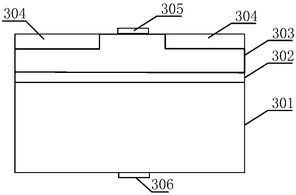
[0041] On the basis of the above embodiments, this embodiment provides a Ge Schottky diode used in a wireless charging receiving circuit, please refer to image 3 , image 3 A schematic structural diagram of a Ge Schottky diode provided by an embodiment of the present invention.

[0042]The Ge Schottky diode provided in this embodiment includes: a semiconductor substrate 301, a Ge buffer layer 302, an epitaxial layer 303, a SiGe layer 304, and a contact electrode 305; wherein, the Ge buffer layer 302, the epitaxial layer 303, and the The SiGe layer 304 is sequentially disposed on the first surface of the semiconductor substrate 301;

[0043] The contact electrode 305 includes a first electrode of a Schottky contact and a second electrode of an ohmic contact, wherein the first electrode is disposed on the surface of the epitaxial layer 303, and the second electrode is disposed on the semiconductor substrate on the second surface of the bottom 301.

[0044] Preferably, the se...


PUM


Abstract

The invention discloses a transceiver circuit for wireless charging and a wireless charging system, the circuit comprises a transmitting circuit (1) and a receiving circuit (2); wherein the transmitting circuit (1) comprises a first capacitor (C1) and a transmitting coil (L1); the receiving circuit (2) comprises a receiving coil (L2), a second capacitor (C2), a third capacitor (C3), a fourth capacitor (C4), a fifth capacitor (C5), a first diode (D1), a second diode (D2), and a third diode (D3). The transceiver circuit of the invention can effectively improve the conversion efficiency of the wireless charging circuit and the device by providing a magnifying rectifying voltage amplifying circuit and a rectifying diode with high mobility. The invention solves the problem of low conversion efficiency of the traditional wireless charging circuit.

Description

technical field [0001] The invention belongs to the technical field of semiconductor integrated circuits, and in particular relates to a transceiver circuit and a wireless charging system for wireless charging. Background technique [0002] Wireless charging technology is a new technology. Compared with the traditional wired charging method, wireless charging is more convenient and safe, especially because it is not limited by wires, chargers, sockets and other factors, wireless charging technology is very convenient to use. [0003] At present, the core issue that limits the large-scale application of wireless charging lies in the efficiency of power conversion, because in the process of wireless charging, the rectification of AC to DC and the inversion of DC to AC, as well as the need for transmission through electromagnetic waves, these processes will inevitably cause energy loss, especially to achieve long-distance high-power wireless magnetoelectric conversion, so the e...

Claims


Application Information

Patent Timeline
Patent Type & Authority Applications(China)
IPC IPC(8): H02J50/10
CPCH02J50/10
Inventor 蒋佳序蒋鹏
Owner XIAN CREATION KEJI CO LTD
Why Eureka
Try Eureka