Method for producing a component carrier, component carrier and semi-finished product

A component-carrying, electronic component technology, applied in printed circuit manufacturing, semiconductor/solid-state device manufacturing, semiconductor/solid-state device components, etc., which can solve problems such as high risk of yield drop, dissipation, and thermal management problems

Active Publication Date: 2021-10-12
AT&S (CHONGQING) CO LTD +1
View PDF3 Cites 0 Cited by
  • Summary
  • Abstract
  • Description
  • Claims
  • Application Information

AI Technical Summary

Problems solved by technology

But in the case of thin core processing, there is a high risk of yield drop with respect to the above process
Furthermore, thermal management is problematic due to the heat generated by the embedded chip
This is especially true in thick core structures where it is more difficult to effectively dissipate the heat generated

Method used


Image

  • Method for producing a component carrier, component carrier and semi-finished product
  • Method for producing a component carrier, component carrier and semi-finished product
  • Method for producing a component carrier, component carrier and semi-finished product

Examples


Embodiment approach

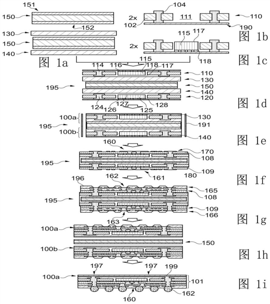
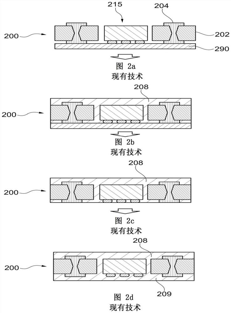
[0079] Fanned out wafer level packaging (FOWLP) is one of the latest packaging trends in microelectronics, according to an exemplary embodiment of the present invention. It has high potential for significant package miniaturization in relation to package volume and its thickness. The core of FOWLP technology is the formation of reconfigured molded wafers bonded to thin film redistribution layers to produce SMD compatible packages. The main advantages of FOWLP are substrateless packages, low thermal resistance, improved RF performance due to shorter interconnects and direct IC connections through thin film metallization instead of wire bonds or flip-chip bumps, and lower parasitics. Especially compared to the FC-BGA package, the inductance of FOWLP is much lower. In addition, the redistribution layer can also provide embedded passive devices and antenna structures using a multilayer structure. It can be used for system-in-package (SiP) and heterogeneously integrated multi-chi...


PUM


Abstract

A method for producing a first component carrier and a second component carrier, a component carrier and a semi-finished product are provided. The method comprises: i) providing a separation member comprising a first separation surface and a second separation surface opposite the first separation surface; ii) coupling a first base structure having a first cavity to the first separation surface; iii) coupling a second base structure having a second cavity with a second separation surface; iv) placing the first electronic component in the first cavity; v) connecting the first base structure with the first electronic component to form a first The component carrier; vi) placing the second electronic component in the second cavity; vii) connecting the second base structure with the second electronic component to form the second component carrier; viii) connecting the first component carrier with the separate component and ix) separating the second part carrier from the second parting surface of the parting part.

Description

technical field [0001] The present invention relates to a method of manufacturing a component carrier, a component carrier and a semi-finished product. Background technique [0002] With the increasing product functionality of component carriers equipped with one or more electronic components, the increasing miniaturization of these electronic components and the increasing number of electronic components to be mounted on component carriers such as printed circuit boards, Increasing adoption of increasingly powerful array-like components or packages with several electronic components having multiple contacts or connections with less and less space between these contacts . The heat generated by such electronic components and the component carriers themselves during removal operations is a growing problem. At the same time, the component carrier should be mechanically robust and electrically reliable in order to be able to operate even under harsh conditions. In particular, ...

Claims


Application Information

Patent Timeline
Patent Type & Authority Patents(China)
IPC IPC(8): H01L23/13H01L23/31H01L23/498H05K3/30
CPCH01L23/13H01L23/3128H01L23/49816H01L23/49822H01L23/49833H05K3/30H01L21/4857H01L21/6835H01L23/5389H01L2221/68345H01L2224/04105H01L2224/12105H01L2224/18H01L2224/2518H05K1/185H05K3/0058H05K3/007H05K3/0097H05K2203/1469H05K2203/1536H01L23/562H05K3/103H05K3/4611
Inventor 睦智秀郑惜金迈克尔·图奥米宁吴昱辉
Owner AT&S (CHONGQING) CO LTD
Why Eureka
Try Eureka