Supercharge Your Innovation With Domain-Expert AI Agents!

Method for preparing epitaxial wafer of light-emitting diode and epitaxial wafer

A technology for light-emitting diodes and epitaxial wafers, which is applied in the field of preparation of epitaxial wafers and epitaxial wafers, can solve the problems of surface warpage of the epitaxial layer, influence the light-emitting uniformity of light-emitting diodes, etc., and achieve the effect of improving the light-emitting uniformity.

Active Publication Date: 2020-12-25
HC SEMITEK ZHEJIANG CO LTD
View PDF10 Cites 0 Cited by
  • Summary
  • Abstract
  • Description
  • Claims
  • Application Information

AI Technical Summary

Problems solved by technology

[0003] Epitaxial wafers are usually grown using Metal-organic Chemical Vapor Deposition (English: Metal-organic Chemical Vapor Deposition, abbreviated: MOCVD) equipment during preparation. There is a turntable in the MOCVD equipment, and a circular disk for placing the substrate is arranged on the turntable. Groove, when preparing the epitaxial wafer, the substrate is placed in the circular groove, and the heat is transferred to the substrate through the contact MOCVD equipment between the substrate and the circular groove. The contact area between the shaped grooves is different, resulting in different temperatures at different positions on the substrate, which in turn causes different thermal stresses at different parts of the epitaxial layer grown on the substrate, and different thermal stresses are generated at different positions on the epitaxial layer Different strains will eventually lead to warpage on the surface of the epitaxial layer, which will affect the uniformity of light emitting diodes

Method used


Image

  • Method for preparing epitaxial wafer of light-emitting diode and epitaxial wafer
  • Method for preparing epitaxial wafer of light-emitting diode and epitaxial wafer
  • Method for preparing epitaxial wafer of light-emitting diode and epitaxial wafer

Examples


Embodiment Construction

[0031] In order to make the object, technical solution and advantages of the present invention clearer, the implementation manner of the present invention will be further described in detail below in conjunction with the accompanying drawings.

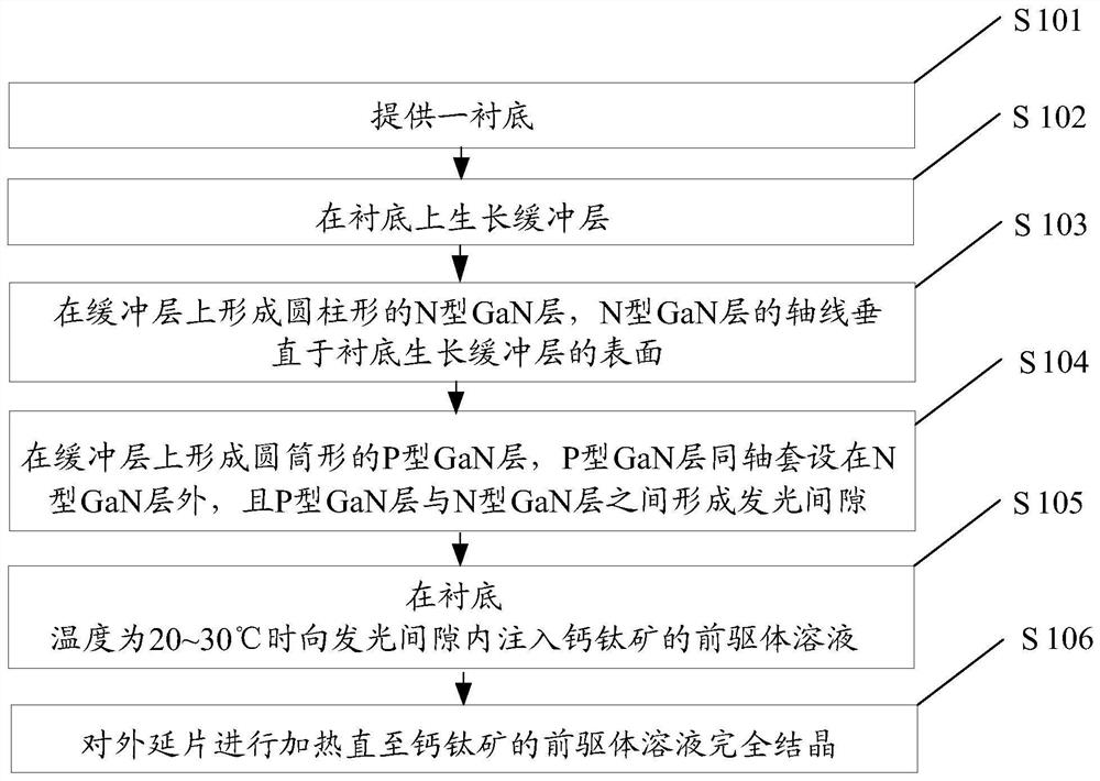
[0032] figure 1 It is a flow chart of a method for preparing an epitaxial wafer of a light-emitting diode provided by an embodiment of the present invention, such as figure 1 Said, the preparation method comprises:

[0033] S101: Provide a substrate.

[0034] S102: growing a buffer layer on the substrate.

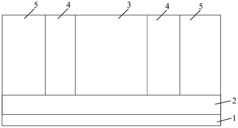
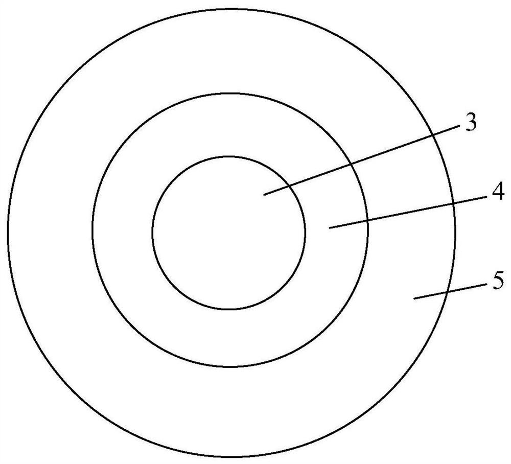
[0035] S103: forming a cylindrical N-type GaN layer on the buffer layer, the axis of the N-type GaN layer being perpendicular to the surface of the substrate where the buffer layer is grown.

[0036] S104: forming a cylindrical P-type GaN layer on the buffer layer, the P-type GaN layer is coaxially sleeved outside the N-type GaN layer, and an annular light-emitting gap is formed between the P-type GaN layer and the N-type GaN lay...


PUM

PropertyMeasurementUnit
diameteraaaaaaaaaa
heightaaaaaaaaaa
thicknessaaaaaaaaaa

Abstract

The invention discloses a preparation method of an epitaxial wafer of a light-emitting diode, and an epitaxial wafer, and belongs to the field of the light-emitting diode manufacturing. The preparation method comprises the following steps: respectively growing coaxial N-type GaN layer and P-type GaN layer on a buffer layer on a substrate, wherein an axis of the N-type GaN layer is vertical to thesurface for growing the buffer layer on the substrate, and a light-emitting gap is formed between the P-type GaN layer and the N-type GaN layer; injecting a precursor solution of perovskite in the light-emitting gap, heating and completely crystalizing the precursor solution in the light-emitting gap, wherein the electron provided by the N-type GaN layer and a cavity provided by the P-type GaN layer are in composite light-emitting in the completely crystallized perovskite. In the forming process of the perovskite, the perovskite is formed through complete crystallization, but not grows throughthe MOCVD equipment; the growth conditions at various places in the perovskite are relatively uniform, the problem that the light-emitting is non-uniform due to nonuniform temperature in the epitaxial wafer is inexistent, and the light-emitting uniformity of the light-emitting diode can be greatly improved.

Description

technical field [0001] The invention relates to the field of light-emitting diode manufacturing, in particular to a method for preparing an epitaxial wafer of a light-emitting diode and the epitaxial wafer. Background technique [0002] Light-emitting diodes are semiconductor diodes that can convert electrical energy into light energy. They have the advantages of small size, long life, and low power consumption. They are currently widely used in automotive signal lights, traffic lights, display screens, and lighting equipment. The epitaxial wafer is the basic structure for making light-emitting diodes. The structure of the epitaxial wafer includes a substrate and an epitaxial layer grown on the substrate. The epitaxial layer includes a buffer layer, an N-type GaN layer, and an InGaN / GaN multi-quantum layer grown on the substrate in sequence. Well layer and P-type GaN layer. [0003] Epitaxial wafers are usually grown using Metal-organic Chemical Vapor Deposition (English: M...

Claims


Application Information

Patent Timeline
Patent Type & Authority Patents(China)
IPC IPC(8): H01L33/00H01L33/12H01L33/32
CPCH01L33/005H01L33/12H01L33/32
Inventor 赵利削郭炳磊吕蒙普胡加辉李鹏
Owner HC SEMITEK ZHEJIANG CO LTD
Features
  • R&D
  • Intellectual Property
  • Life Sciences
  • Materials
  • Tech Scout
  • Unparalleled Data Quality
  • Higher Quality Content
  • 60% Fewer Hallucinations
Learn More