High-electron-mobility transistor and preparation method thereof

A technology with high electron mobility and transistors, which is applied in semiconductor/solid-state device manufacturing, circuits, electrical components, etc., can solve problems such as high electron concentration, achieve the effects of reducing power consumption, enhancing breakdown resistance, and enhancing mobility

Inactive Publication Date: 2019-04-19
HC SEMITEK ZHEJIANG CO LTD
View PDF0 Cites 0 Cited by
  • Summary
  • Abstract
  • Description
  • Claims
  • Application Information

AI Technical Summary

Problems solved by technology

[0006] The embodiment of the present invention provides a high electron mobility transistor and its preparation method, which can solve the problem that the high concentration of electrons in the channel layer in the prior art affects the heterogeneity of the channel layer (GaN) and the barrier layer (AlGaN) The problem of forming a high-concentration, high-mobility two-dimensional electron gas at the junction interface

Method used


Image

  • High-electron-mobility transistor and preparation method thereof
  • High-electron-mobility transistor and preparation method thereof
  • High-electron-mobility transistor and preparation method thereof

Examples


Embodiment Construction

[0033] In order to make the object, technical solution and advantages of the present invention clearer, the implementation manner of the present invention will be further described in detail below in conjunction with the accompanying drawings.

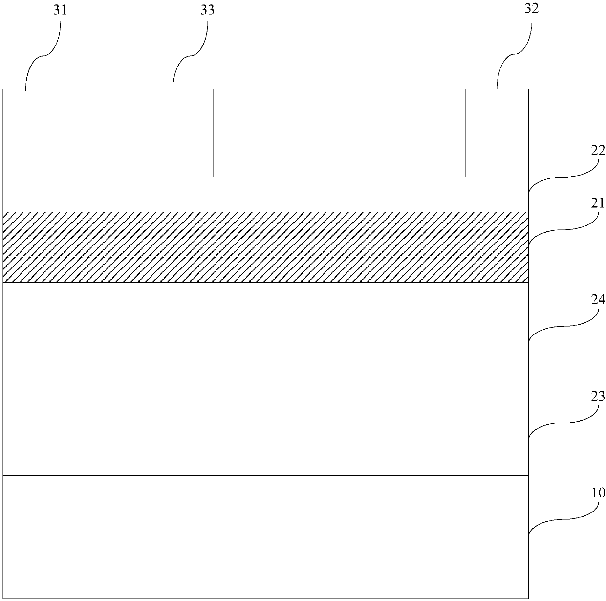
[0034] An embodiment of the present invention provides a high electron mobility transistor. figure 1 A schematic structural diagram of a high electron mobility transistor provided by an embodiment of the present invention. see figure 1 , the high electron mobility transistor comprises a substrate 10, a channel layer 21, a barrier layer 22, a source 31, a drain 32 and a gate 33, and the channel layer 21 and the barrier layer 22 are sequentially stacked on the substrate 10 , the source 31 , the drain 32 and the gate 33 are respectively disposed on the barrier layer 22 . Both the source 31 and the drain 32 form ohmic contacts with the barrier layer 22 , and the gate 33 forms a Schottky contact with the barrier layer 22 .

[0035] fig...


PUM


Abstract

The invention discloses a high-electron-mobility transistor and a preparation method thereof, which belongs to the technical field of semiconductors. The high-electron-mobility transistor comprises asubstrate, a channel layer, a barrier layer, a source, a drain and a gate, wherein the channel layer and the barrier layer are sequentially laminated on the substrate, the source, the drain and the gate are arranged on the barrier layer respectively, both the source and the drain form an ohmic contact with the barrier layer, and the gate and the barrier layer forms a Schottky contact; and the channel layer comprises a first sub-layer and a second sub-layer inserted into the first sub-layer, the first sub-layer is an undoped GaN layer, and the second sub-layer is an Au/Ag nanoparticle layer. Through inserting the Au/Ag nanoparticle layer into the undoped GaN layer, the formation of a two-dimensional electronic gas with high concentration and high mobility at a heterojunction interface of the channel layer (GaN) and the barrier layer (AlGaN) is facilitated.

Description

technical field [0001] The invention relates to the technical field of semiconductors, in particular to a high electron mobility transistor. Background technique [0002] A high electron mobility transistor (English: High electron mobility transistor, HEMT for short) is a type of field effect transistor, which uses two materials with different energy gaps to form a heterojunction to provide a channel for carriers. Gallium nitride (GaN)-based materials have the characteristics of wide band gap, high electron mobility, high voltage resistance, radiation resistance, easy formation of heterostructures, and large spontaneous polarization effect, and are suitable for the preparation of new generation high-frequency high-power microelectronic devices such as HEMTs and circuits. At present, GaN-based materials and devices are the frontier and hotspot in the global semiconductor field, and have great application prospects in the military and civilian fields. [0003] Existing high ...

Claims


Application Information

Patent Timeline
Patent Type & Authority Applications(China)
IPC IPC(8): H01L29/778H01L21/335
CPCH01L29/7786H01L29/66462
Inventor 葛永晖郭炳磊王群吕蒙普李鹏
Owner HC SEMITEK ZHEJIANG CO LTD
Why Eureka
Try Eureka