Method for chemically plating metal on copper substrate and printed circuit board and wafer prepared by same

A copper substrate and electroless plating technology, applied in the field of electroless metal plating, can solve the problems of unfriendly environment, influence of coating reliability, influence of bonding force between coating and base material, etc.

Active Publication Date: 2019-04-19
GUANGDONG TONESET SCI & TECH
View PDF4 Cites 1 Cited by
  • Summary
  • Abstract
  • Description
  • Claims
  • Application Information

AI Technical Summary

Problems solved by technology

Among them, if the pre-dip formula is adjusted in method (1), it is often necessary to add special additives. The added additives may affect the bonding force between the subsequent coating and the substrate, or there are problems such as environmental unfriendliness. conditions, such as lowering the temperature of the activation tank, the stabili

Method used


Image

  • Method for chemically plating metal on copper substrate and printed circuit board and wafer prepared by same
  • Method for chemically plating metal on copper substrate and printed circuit board and wafer prepared by same
  • Method for chemically plating metal on copper substrate and printed circuit board and wafer prepared by same

Examples


Embodiment 1

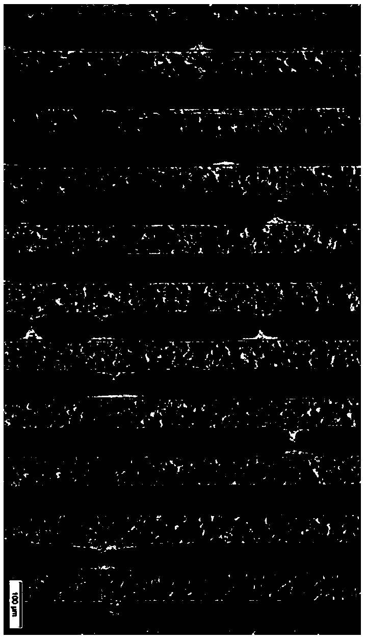
[0038] Embodiment 1 Immersion nickel gold on the printed circuit board

[0039] Process flow: degreasing→water washing→micro-etching→water washing→presoaking→activation→water washing→immersion nickel→water washing→immersion gold→water washing→drying

[0040] (1) Degreasing: Use TS-Acidclean 6189 degreasing agent from Guangdong Dongshuo Technology Co., Ltd., the operating temperature is 35°C, and the treatment time is 5 minutes.

[0041] (2) Microetching: The microetching agent is composed of 100 g / L sodium persulfate and 2% (v / v) sulfuric acid, the operating temperature is 30° C., and the treatment time is 2 minutes.

[0042] (3) Pre-soaking: 1% sulfuric acid is used for treatment, and a water bath jacket is installed outside the pre-soaking tank so that the temperature of the pre-soaking tank can be reduced to 20° C., and the treatment time is 2 minutes.

[0043] (4) Activation: use the TS-Activator LA activation solution produced by Guangdong Dongshuo Technology Co., Ltd., ...

Embodiment 2

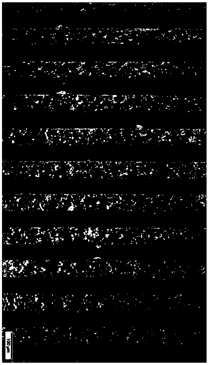
[0047] Embodiment 2 Immersion nickel gold on the printed circuit board

[0048] Process flow: degreasing→water washing→micro-etching→water washing→presoaking→activation→water washing→immersion nickel→water washing→immersion gold→water washing→drying

[0049] (1) Degreasing: Use TS-Acidclean 6189 degreasing agent from Guangdong Dongshuo Technology Co., Ltd., the operating temperature is 35°C, and the treatment time is 5 minutes.

[0050] (2) Microetching: The microetching agent is composed of 100 g / L sodium persulfate and 2% (v / v) sulfuric acid, the operating temperature is 30° C., and the treatment time is 2 minutes.

[0051] (3) Pre-soaking: 1% sulfuric acid is used for treatment, and a water bath jacket is installed outside the pre-soaking tank so that the temperature of the pre-soaking tank can be reduced to 15° C., and the treatment time is 2 minutes.

[0052] (4) Activation: use the TS-Activator LA activation solution produced by Guangdong Dongshuo Technology Co., Ltd., ...

Embodiment 3

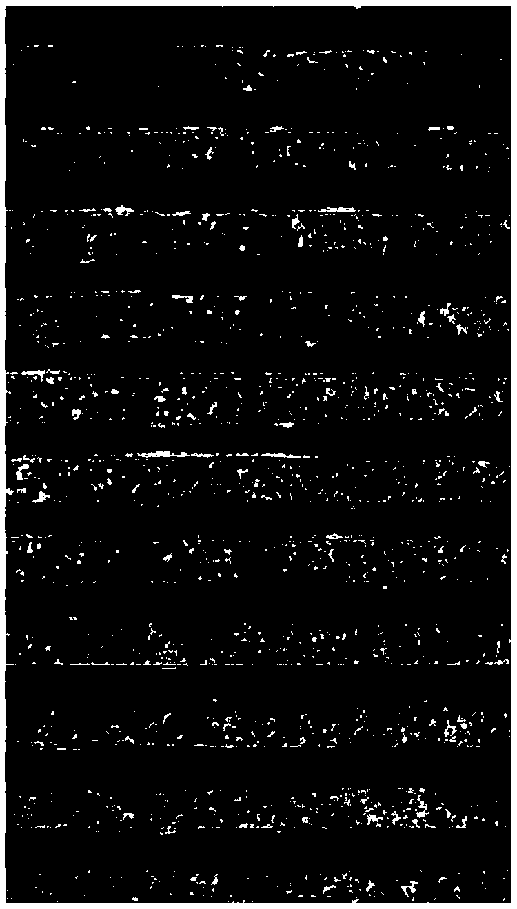
[0056] Embodiment 3 Immersion nickel gold on the printed circuit board

[0057] Process flow: degreasing→water washing→micro-etching→water washing→presoaking→activation→water washing→immersion nickel→water washing→immersion gold→water washing→drying

[0058] (1) Degreasing: Use TS-Acidclean 6189 degreasing agent from Guangdong Dongshuo Technology Co., Ltd., the operating temperature is 35°C, and the treatment time is 5 minutes.

[0059] (2) Microetching: The microetching agent is composed of 100 g / L sodium persulfate and 2% (v / v) sulfuric acid, the operating temperature is 30° C., and the treatment time is 2 minutes.

[0060] (3) Pre-soaking: 1% sulfuric acid is used for treatment, and a water bath jacket is installed outside the pre-soaking tank, so that the temperature of the pre-soaking tank can be reduced to 8° C., and the treatment time is 2 minutes.

[0061] (4) Activation: use the TS-Activator LA activation solution produced by Guangdong Dongshuo Technology Co., Ltd., ...


PUM


Abstract

The invention relates to a method for chemically plating metal on a copper substrate, a printed circuit board and a wafer prepared by the method. The method for chemically plating metal on the coppersubstrate comprises the following steps: oil removal, micro-etching, preimpregnation, activation and chemical metal plating; and the surface temperature of the printed circuit board being reduced to below 20 DEG C before the step of activation. According to the method, diffusion coating phenomenon is effectively prevented on the basis of not changing the formula of a bath solution in each step inan existing process.

Description

technical field [0001] The invention relates to the technical field of electroless metal plating, in particular to a method for electroless metal plating on a copper substrate and a printed circuit board and wafer prepared therefrom. Background technique [0002] With the continuous development of electronic products, the circuit design of its electrical components is becoming more and more complex. Complex printed circuit boards or wafers require more functions in the final surface treatment process, and higher and higher flatness requirements. The chemical nickel-gold or nickel-palladium-gold process integrates solderability, contact conductivity, wire bonding and heat dissipation, and has become the surface of copper substrates on printed circuit boards or wafers (mainly composed of silicon). One of the mainstream of processing. [0003] The chemical nickel-gold process generally includes the following steps: degreasing, micro-etching, pre-dipping, activation, post-dippi...

Claims


Application Information

Patent Timeline
IPC IPC(8): H05K3/24
CPCH05K3/24
Inventor 李小兵黎小芳张俊林
Owner GUANGDONG TONESET SCI & TECH
Why Eureka
Try Eureka