Supercharge Your Innovation With Domain-Expert AI Agents!

Method of manufacturing semiconductor devices

A production method and semiconductor technology, applied in the fields of semiconductor devices, semiconductor/solid-state device manufacturing, electric solid-state devices, etc., can solve the problem of reducing the absolute accuracy of resistance value, preventing extensive miniaturization, and reducing the concentration and resistance value of resistance element diffusion layer. Small and other problems, to achieve the effect of easy control, high integration and remarkable effect

Inactive Publication Date: 2002-12-18
NEC ELECTRONICS CORP
View PDF4 Cites 0 Cited by
  • Summary
  • Abstract
  • Description
  • Claims
  • Application Information

AI Technical Summary

Problems solved by technology

However, when the base diffusion layer of the bipolar element and the diffusion layer of the resistance element are to be formed at the same time, the concentration of the diffusion layer of the resistance element is necessarily increased while causing a decrease in the magnitude of the resistance
When the resistive element is formed with a smaller width or greater length than is generally desired at a reduced magnitude of resistance, the reduced width reduces the absolute accuracy of the magnitude of resistance or the increased length prevents widespread miniaturization of the element

Method used


Image

  • Method of manufacturing semiconductor devices
  • Method of manufacturing semiconductor devices
  • Method of manufacturing semiconductor devices

Examples


Embodiment Construction

[0026] Several preferred embodiments of the present invention will now be described with reference to the accompanying drawings.

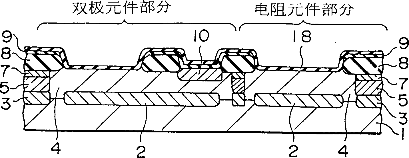
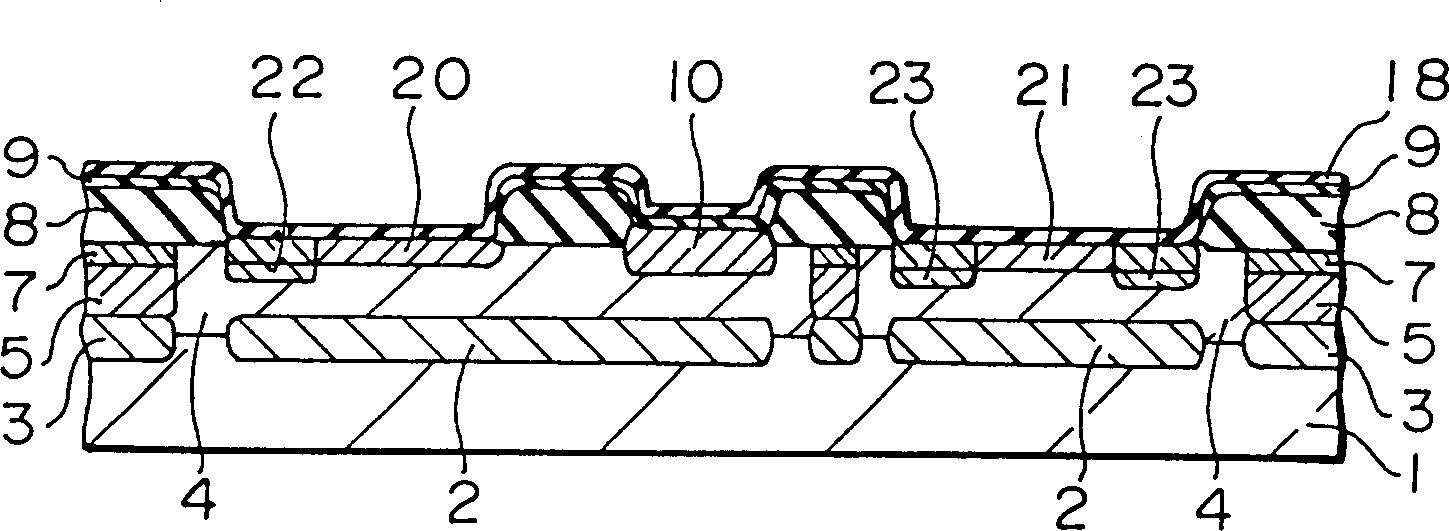
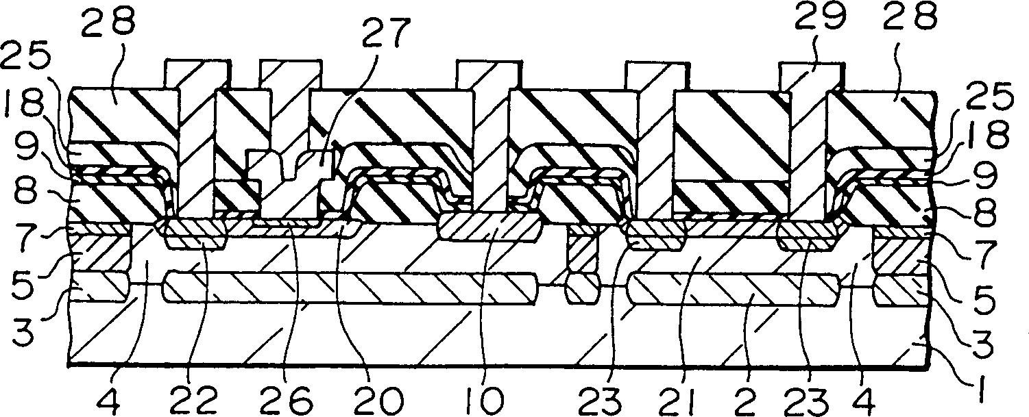
[0027] Figures 2A-2C is a sectional view sequentially showing the main constituent steps of the first preferred embodiment of the present invention. On the P-type silicon substrate 1, -N+ type embedded layer 2 and -P+ type embedded layer 3 are formed, followed by growing an N-type epitaxial layer 4 with a thickness of 1.0-3.0 microns, and -P-type well 5, A P-type channel stopper ring 7 and a field oxide film 8 are formed. Then, in an oxygen environment at a temperature of 900-1000° C., the total surface produced by oxidation is a thickness of 200 Å, forming the first oxide film 9, and passing through the partial collector region of the bipolar element at a thickness of about 1-2× 10 16 cm -2 Phosphorus is ion-implanted to form the -N+ type collector diffusion layer 10 . Up to the above step, the current method is the same as the conventional ...


PUM


Abstract

A method for producing a semiconductor device provided on a silicon substrate with a bipolar element portion and a resistive element portion formed by an impurity diffusion layer, comprising: (a) on the silicon substrate and on the entire surface of the substrate A step of forming a first oxide film on the constituent elements formed above; (b) selectively and sequentially removing the part of the base region corresponding to the bipolar element and the silicon substrate directly under the first oxide film The first oxide film portion and the step of cleaning the newly exposed surface; (c) forming a second oxide film on the silicon substrate and the constituent elements formed on the entire surface thereof, wherein the oxide film thickness on the base region and the resistance region There are differences; (d) the step of selectively and momentarily implanting ions into said bipolar element and resistive element portions.

Description

technical field [0001] The present invention relates to a method for producing a semiconductor device consisting of an integrated circuit having a bipolar element and a resistance element or a dual CMOS integrated circuit having a bipolar element and a MOS device combined in a mixed state therein . Background technique [0002] Conventional circuits with a bipolar element must have a high precision resistive device, which is usually formed simultaneously with the base diffusion layer of the bipolar element. For example, the disclosed technology about this configuration is "Ultrafast Digital Devices", Vol. 1, "Ultrafast Bipolar Devices", Section 4.4.1, pp. 90-91, published by BaiFukan. [0003] The following will be combined with Figures 1A to 1C , presents a method of producing a conventional semiconductor device integrated circuit having a bipolar element and a resistive element. - N+ type embedded layer 2 and a P+ type embedded layer 3 are respectively formed on a P typ...

Claims


Application Information

Patent Timeline
Patent Type & Authority Patents(China)
IPC IPC(8): H01L21/265H01L21/331H01L21/8222H01L21/8249H01L27/06H01L29/73H01L29/732
CPCH01L21/8222H01L27/0658Y10S148/163Y10S148/136
Inventor 若林胜
Owner NEC ELECTRONICS CORP
Features
  • R&D
  • Intellectual Property
  • Life Sciences
  • Materials
  • Tech Scout
  • Unparalleled Data Quality
  • Higher Quality Content
  • 60% Fewer Hallucinations
Learn More