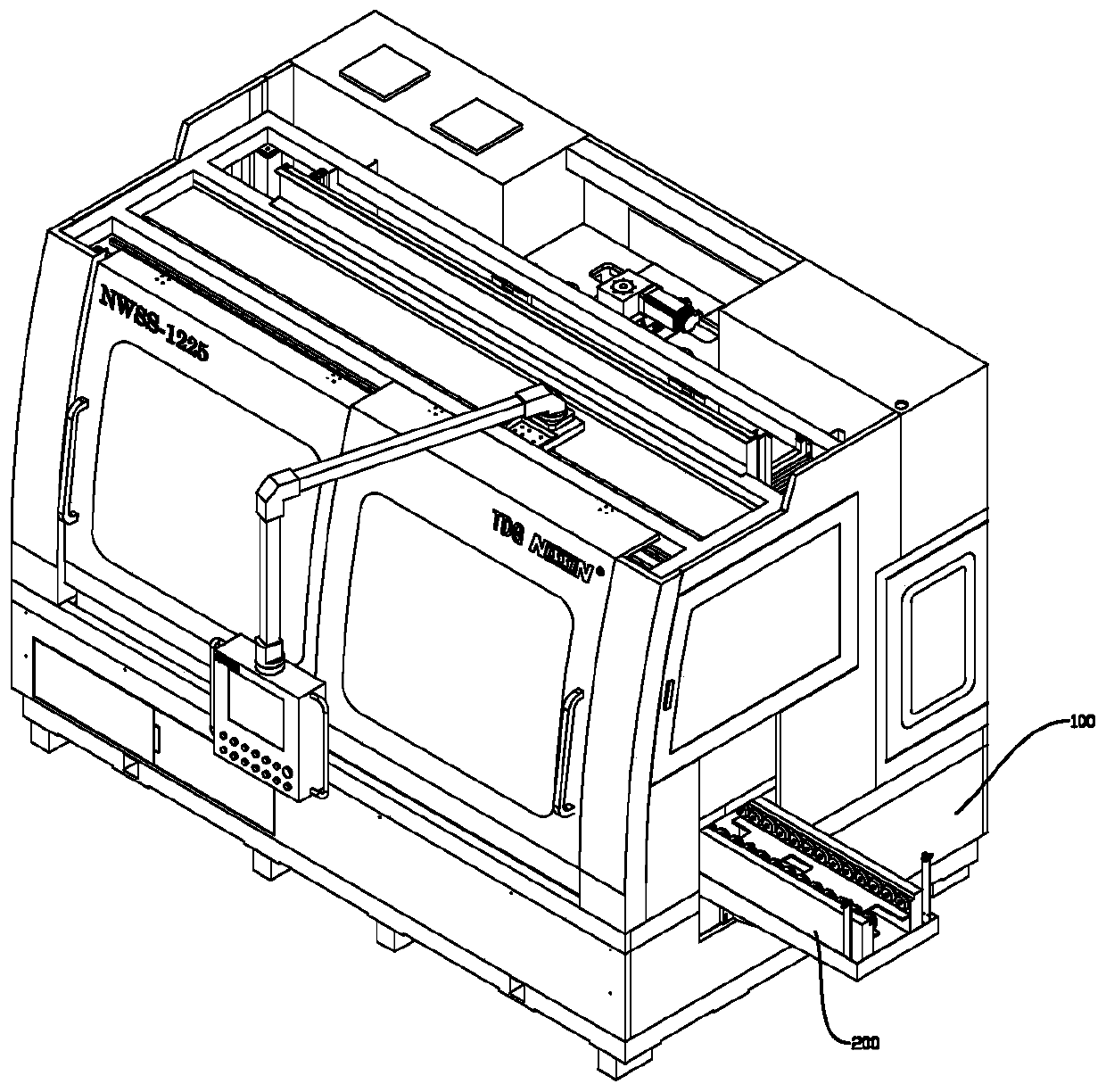
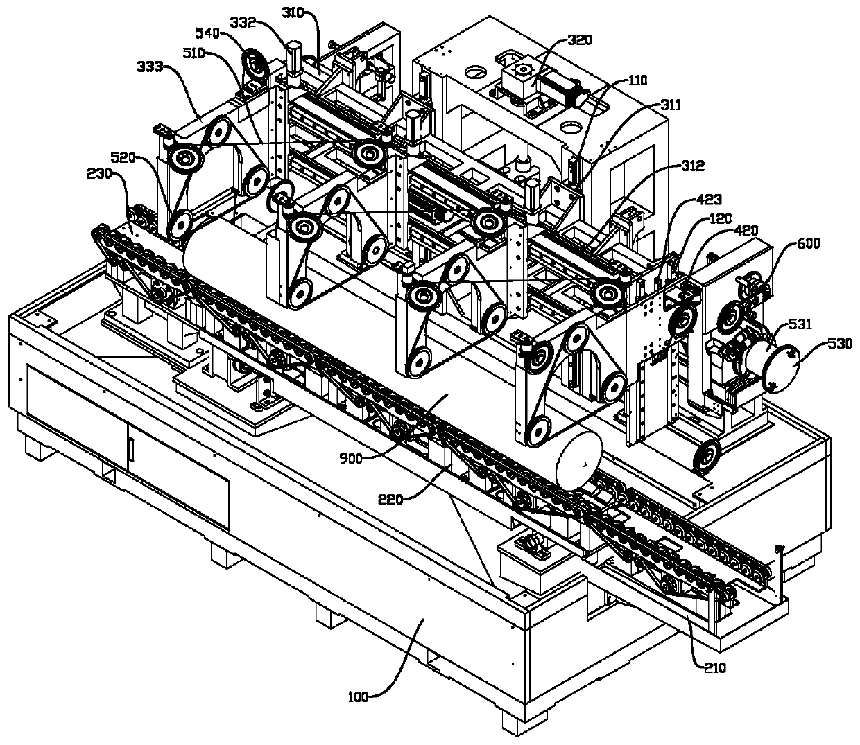
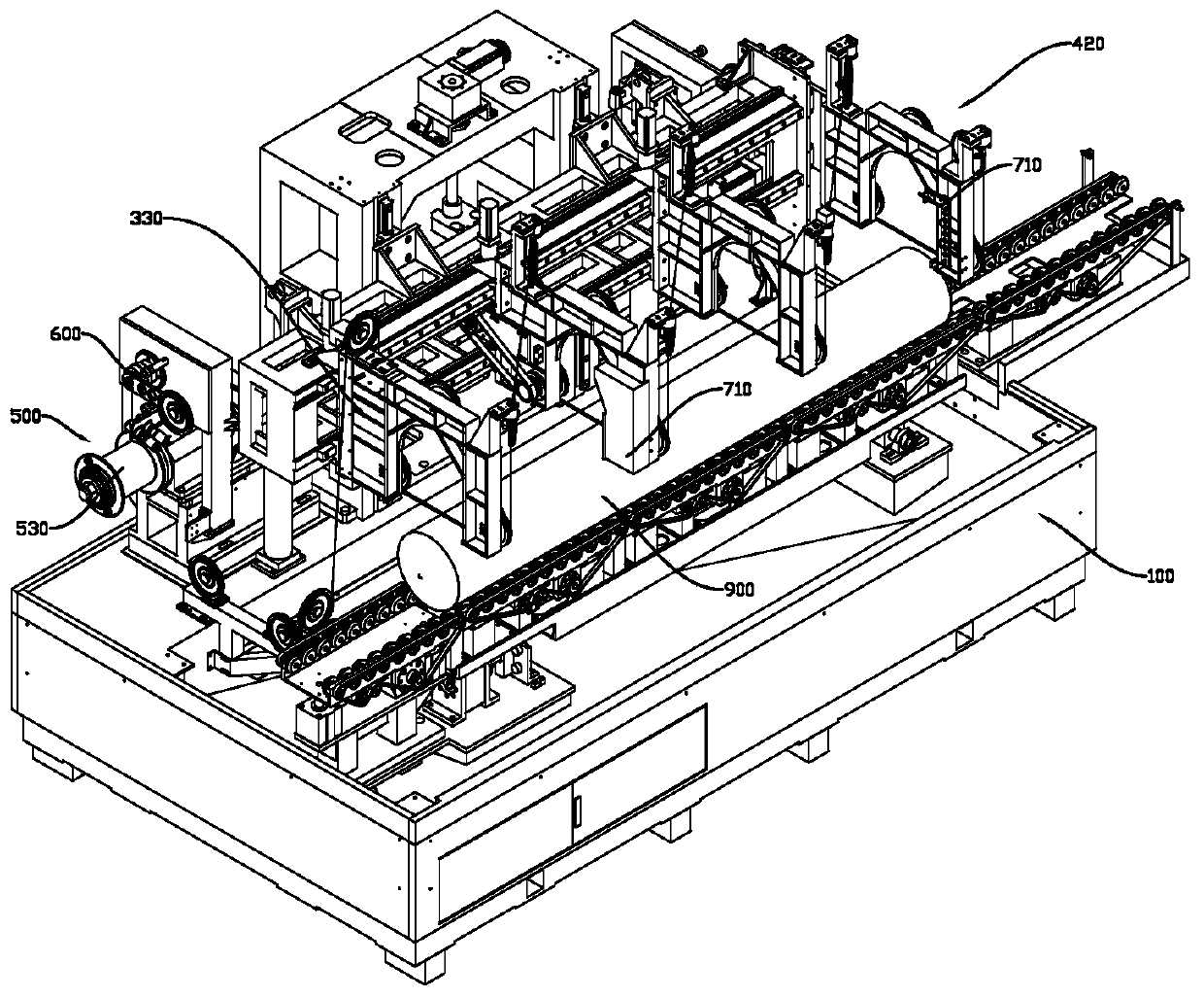
Crystal bar cutoff method of multi-stage semiconductor crystal bar cutoff machine

A semiconductor, multi-stage technology, applied in the direction of fine work equipment, work accessories, stone processing equipment, etc., can solve the problems of single cutting function, low efficiency, and can not meet various requirements. Functional single effect

Active Publication Date: 2019-05-21
TDG NISSIN PRECISION MACHINERY CO LTD
View PDF8 Cites 4 Cited by
  • Summary
  • Abstract
  • Description
  • Claims
  • Application Information

AI Technical Summary

Problems solved by technology

[0003] However, there are still deficiencies in current semiconductor ingot cutting machines. For example, the existing semiconductor ingot cutting machines often have a single cutting function and cannot adapt to the ingot cutting processing of various requirements; in addition, the existing semiconductor ingot cutting machines Before the workpiece is processed, it often lacks the leveling function of the workpiece, resulting in that after the semiconductor crystal rod is cut off, due to the uniformity of the semiconductor crystal rod itself, there is a gap between the truncated surface at both ends and the longitudinal center axis of the semiconductor crystal rod itself. Not vertical enough
And the error is passed into the subsequent ingot rounding, so that the effective utilization rate of the semiconductor ingot is greatly reduced
At the same time, in the process of cutting the crystal ingot and sampling the existing semiconductor ingot cutting machine, when it is necessary to intercept multiple test samples at one semiconductor ingot cutoff, it often needs to be cut through multiple cuts. The way the process is lengthy and inefficient

Method used


Image

  • Crystal bar cutoff method of multi-stage semiconductor crystal bar cutoff machine
  • Crystal bar cutoff method of multi-stage semiconductor crystal bar cutoff machine
  • Crystal bar cutoff method of multi-stage semiconductor crystal bar cutoff machine

Examples


Embodiment Construction

[0061] Embodiments of the present invention are described in detail below, examples of which are illustrated in the accompanying drawings, wherein the same or similar reference numerals refer to the same or similar elements or elements having the same or similar functions throughout. The embodiments described below with reference to the accompanying drawings are exemplary, only used to explain the present invention, and should not be construed as a limitation of the present invention.

[0062] In the description of the present invention, it should be understood that the terms "center", "longitudinal", "lateral", "length", "width", "thickness", "upper", "lower", "front", " rear, left, right, vertical, horizontal, top, bottom, inside, outside, clockwise, counterclockwise, etc., or The positional relationship is based on the orientation or positional relationship shown in the accompanying drawings, which is only for the convenience of describing the present invention and simplify...


PUM


Abstract

The invention discloses a crystal bar cutoff method of a multi-stage semiconductor crystal bar cutoff machine. The crystal bar cutoff method comprises the steps that S1, a feeding device is used for transferring a semiconductor crystal bar to be cut onto a feeding platform of a material conveying device, and the feeding platform feeds the semiconductor crystal bar to a cutting platform and enablesthe semiconductor crystal bar to fall onto the cutting platform; S2, an aligning device adjusts the level condition of the center axis of the semiconductor crystal bar on the cutting platform; S3, the semiconductor crystal bar is subjected to cutting and sampling operation in cutoff positions in multiple cutting modes; and S4, cutoff crystal bar sections are fed into a discharging platform from the cutting platform in sequence and finally discharged from the discharging platform into a transfer device. Through cooperation of the above method and the multi-stage semiconductor crystal bar cutoff machine, the problems that the cutting functionality is single in the crystal bar section cutoff process, the perpendicularity of the cutoff end face to the center axis of crystal bar sections is poor, the sampling efficiency is low and the crystal bar sections are damaged easily in the conveying process in the prior art are effectively solved.

Description

technical field [0001] The invention relates to a method for cutting semiconductor crystal rods, in particular to a crystal rod cutting method using a multi-segment semiconductor crystal rod cutting machine. Background technique [0002] Wire cutting technology is currently the most advanced semiconductor crystal rod cutting machine in the world. Its principle is to process workpieces (such as single crystal silicon rods, sapphire or other semiconductor brittle and hard materials) required by reciprocating friction of diamond wire running at high speed. The surface is rubbed, and a semiconductor crystal rod with a long length is truncated into a crystal rod with a shorter length, so as to facilitate the next rounding of the crystal rod. During the truncation of the semiconductor ingot, the diamond wire is guided by the wire wheel to form a wire mesh on the main wire roller, and the workpiece to be processed is fed by the rise and fall of the worktable. Under the action of th...

Claims


Application Information

Patent Timeline
IPC IPC(8): B28D5/04B28D7/00
Inventor 卢建伟苏静洪裴忠张峰李鑫潘雪明曹奇峰
Owner TDG NISSIN PRECISION MACHINERY CO LTD
Why Eureka
Try Eureka