A wafer level packaging method of an MEMS device

A technology of wafer-level packaging and devices, applied in semiconductor/solid-state device parts, piezoelectric/electrostrictive/magnetostrictive devices, instruments, etc., can solve the problems of increasing the damage probability of MEMS devices, and reach the optional range Wide, reduce the damage probability, reduce the effect of package cost

Inactive Publication Date: 2019-05-28
RDA MICROELECTRONICS SHANGHAICO LTD
View PDF10 Cites 4 Cited by
  • Summary
  • Abstract
  • Description
  • Claims
  • Application Information

AI Technical Summary

Problems solved by technology

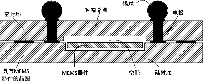
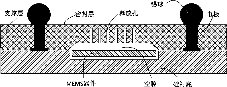
The solution is to manufacture a packaging structure formed by two layers of polymer films on the wafer where the MEMS device is located. On the one hand, the entire process will greatly increase the damage probability of the MEMS device. On the other hand, in order to reduce the damage to the MEMS device, it is necessary to The material and release process of the polymer film have strict restrictions

Method used


Image

  • A wafer level packaging method of an MEMS device
  • A wafer level packaging method of an MEMS device
  • A wafer level packaging method of an MEMS device

Examples


Embodiment Construction

[0028] see Figure 4 , Embodiment 1 of the MEMS device wafer-level packaging method of the present application includes the following steps.

[0029] Step 401, such as Figure 5A As shown, a layer of temporary bonding material 102 is deposited on the carrier wafer 101 . Wafer 101 is a wafer for carrying a package structure, without MEMS devices thereon. Preferably, the carrier wafer 101 can be made of single crystal silicon, glass and other materials. Preferably, the temporary bonding material 102 is thermally sensitive, photosensitive, or easily corroded by chemicals, so that the packaging structure can be effectively peeled off from the carrier wafer 101 during subsequent processes. The deposition process is also called a deposition process, preferably chemical vapor deposition (CVD), physical vapor deposition (PVD), etc., and can also be in the form of spin coating or bonding.

[0030] Step 402, such as Figure 5B As shown, a first layer of polymer 103 for making a pac...


PUM


Abstract

The invention discloses a wafer level packaging method of an MEMS device. Firstly, an MEMS device is manufactured on an MEMS wafer, and a packaging structure is attached to a bearing wafer through a temporary bonding material. Secondly, the packaging structure on the bearing wafer and the MEMS wafer are bonded together, and the MEMS device is enclosed by the packaging structure and the MEMS waferin a sealed mode; Thirdly, the temporary bonding material is removed, so that the bearing wafer is stripped from the packaging structure, and packaging of the MEMS device is completed. According to the invention, the manufacturing process of the packaging structure does not influence or damage the MEMS device, the damage probability of the MEMS device in the packaging process is reduced, the optional range of the packaging material is wide, and the packaging cost is reduced.

Description

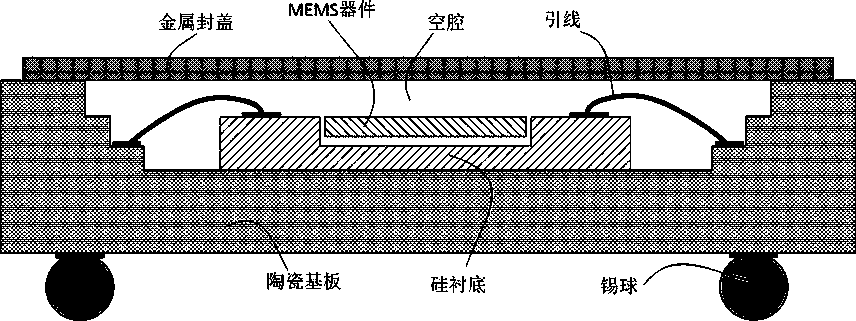
technical field [0001] The present application relates to a wafer level packaging (WLP, Wafer Level Package) method, in particular to a wafer level packaging method for MEMS (Micro Electro Mechanical System, Micro Electro Mechanical System) devices. Background technique [0002] A MEMS device is a microelectronic device with a mechanically movable structure, which is used to convert electrical signals into physical signals such as displacement, velocity, vibration, and sound waves, and can also convert these physical signals into electrical signals. Mechanically movable structures in MEMS devices are typically between a few micrometers and hundreds of micrometers. At this geometric scale, mechanically movable structures are easily disturbed and damaged by dust, moisture, and volatile chemicals in the environment. For example, dust with large particles in the environment is deposited into the gaps of the mechanically movable structure of the MEMS device, causing failure of t...

Claims


Application Information

Patent Timeline
Patent Type & Authority Applications(China)
IPC IPC(8): B81B7/02B81C3/00
Inventor 冯端李平胡念楚贾斌
Owner RDA MICROELECTRONICS SHANGHAICO LTD
Why Eureka
Try Eureka