Wideband power amplifiers with harmonic traps

A technology of amplifiers and wave traps, which is applied in the field of packaged semiconductor devices, can solve the problems of no longer constant base load, increased interaction sensitivity, and limited PA bandwidth, etc.

Active Publication Date: 2019-05-28
NXP USA INC
View PDF18 Cites 10 Cited by
  • Summary
  • Abstract
  • Description
  • Claims
  • Application Information

AI Technical Summary

Problems solved by technology

Specifically, the frequency dispersion introduced at both ends of the harmonic frequency band of the Doherty PA causes (i) increased sensitivity to the interaction between the fundamental matching impedance and the harmonic termination and (ii) an optimal fundamental at the output of the PA. The load is no longer constant, which effectively limits the PA bandwidth

Method used


Image

  • Wideband power amplifiers with harmonic traps
  • Wideband power amplifiers with harmonic traps
  • Wideband power amplifiers with harmonic traps

Examples


Embodiment Construction

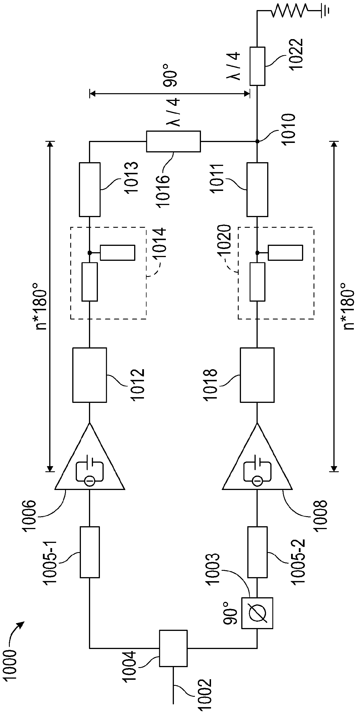
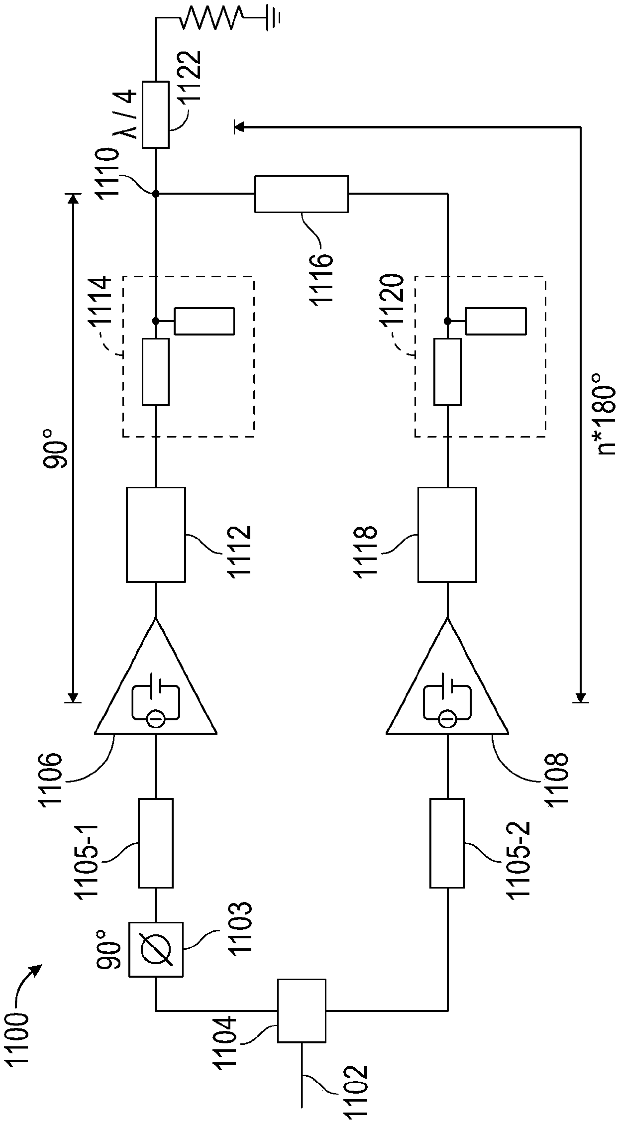
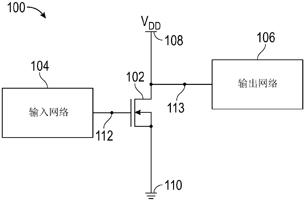
[0076] Before any embodiments of the invention are explained in detail, it is to be understood that the invention in its application is not limited to the details of construction and the arrangement of parts set forth in the following description or shown in the following drawings. The invention is capable of other embodiments and of being practiced or carried out in various ways. Also, it is to be understood that the phraseology and terminology used herein are for the purpose of description and should not be regarded as limiting. Use of "including," "including," or "having" and variations thereof herein is intended to encompass the items listed thereafter and equivalents thereof as well as additional items. Unless otherwise specified or limited, the terms "mount", "connect", "support" and "couple" and variations thereof are used broadly and encompass direct and indirect mounting, connection, support and coupling. Additionally, "connected" and "coupled" are not limited to phy...


PUM


Abstract

The disclosure relates to wideband power amplifiers with harmonic traps. An amplifier may include a transistor and input and output matching networks. One or more harmonic trap circuits may be electrically connected to a node located between the input matching network and a gate terminal of the transistor or to a node located between the output matching network and a drain terminal of the transistor. Each harmonic trap may provide a low-resistance path to ground for signal energy above a fundamental operating frequency of the amplifier, such as harmonic frequencies thereof. The output matchingnetwork may act as an impedance inverter that provides a 90-degree insertion phase between the input of the output matching network and the load. A variable length drain feeder may connect a voltagesource to an output of the output matching network.

Description

technical field [0001] Embodiments of the subject matter herein relate generally to packaged semiconductor devices, and more particularly to packaged radio frequency (RF) semiconductor devices having impedance matching circuits including harmonic traps for potentially enhanced performance. Background technique [0002] A typical high power radio frequency (RF) semiconductor device may include one or more input leads, one or more output leads, one or more transistors, coupling the one or more input leads to the one or more Bond wires for a plurality of transistors, and bond wires coupling the one or more transistors to the one or more output leads. Bond wires have inductance at high frequencies, and the design of the device's input and output impedance matching circuits takes this inductance into account. In some cases, the input and output impedance matching circuits may be contained within the same package that contains one or more transistors of the device. More specific...

Claims


Application Information

Patent Timeline
Patent Type & Authority Applications(China)
IPC IPC(8): H03F1/02H03F1/56H03F3/193H03F3/21
CPCH03F1/483H03F1/565H03F3/195H03F3/245H03F2200/222H03F2200/36H03F2200/387H03F1/0288H01L28/40H01L2224/49175H01L23/66H01L2223/6655H03F1/56H03F3/213H03F3/60H03F2200/451H01L23/49838H01L29/2003H01L2223/6611H03F1/486H03F3/601H03F2200/255H03F2200/423
Inventor R·麦克拉恩R·斯里尼迪安巴尔
Owner NXP USA INC
Why Eureka
Try Eureka