Semiconductor structures and methods of forming them

A semiconductor and bonding technology, used in semiconductor devices, semiconductor/solid-state device manufacturing, electrical components, etc., can solve problems such as poor transistor performance, achieve good interface state, improve service life, and reduce instability.

Active Publication Date: 2021-12-14
SEMICON MFG INT (SHANGHAI) CORP +1
View PDF4 Cites 0 Cited by
  • Summary
  • Abstract
  • Description
  • Claims
  • Application Information

AI Technical Summary

Problems solved by technology

[0004] However, existing FinFETs perform poorly

Method used


Image

  • Semiconductor structures and methods of forming them
  • Semiconductor structures and methods of forming them
  • Semiconductor structures and methods of forming them

Examples


Embodiment Construction

[0032] As mentioned in the background, the performance of the P-type FinFET is poor.

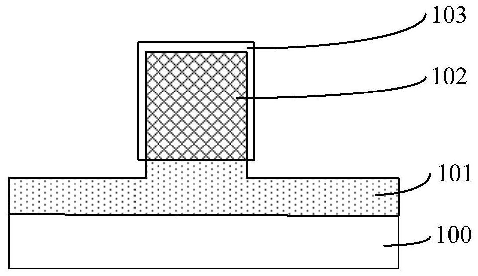
[0033] figure 1 It is a schematic diagram of the structure of a P-type fin field effect transistor.

[0034] Please refer to figure 1 , a substrate 100, the substrate 100 has an insulating layer 101 thereon, and the insulating layer 101 has a fin 102 thereon; an interface layer 103 covering the sidewall and top surface of the fin 102.

[0035] In the above P-type FinFET structure, in order to improve the carrier mobility in the channel region of the P-type FinFET, silicon germanium is used as the material of the fin portion 102 . The carrier mobility is closely related to the concentration of germanium atoms. Specifically, when the atomic percentage concentration of the germanium atoms is less than 25%, the carrier mobility is low, which is not conducive to improving the electrical performance of the P-type fin field effect transistor; on the contrary, when the atomic percentage concentra...


PUM

PropertyMeasurementUnit
thicknessaaaaaaaaaa
thicknessaaaaaaaaaa
thicknessaaaaaaaaaa

Abstract

A semiconductor structure and a method of forming the same, wherein the method includes: providing a substrate having an initial fin on the substrate, the initial fin having a first atom and a second atom therein; and performing a concentration process on the top of the initial fin , forming a fin and a first material layer on the fin, the second atoms in the fin have a first atomic percent concentration, the second atoms in the first material layer have a second atomic percent concentration, and the second atomic percent concentration is greater than The first atomic percentage concentration, and the binding force between the second atom and the oxygen atom is greater than the binding force between the first atom and the oxygen atom; the sidewall of the fin, and the sidewall and top surface of the first material layer are oxidized to form interface layer. The performance of the transistor formed by the method is relatively stable and the service life is long.

Description

technical field [0001] The invention relates to the field of semiconductor manufacturing, in particular to a semiconductor structure and a forming method thereof. Background technique [0002] With the rapid development of semiconductor manufacturing technology, semiconductor devices are developing toward higher component density and higher integration. As the most basic semiconductor device, transistors are currently being widely used. Therefore, as the component density and integration of semiconductor devices increase, the gate size of planar transistors is getting shorter and shorter. The control ability of traditional planar transistors on channel current Weakened, resulting in short channel effect, resulting in leakage current, and ultimately affecting the electrical performance of semiconductor devices. [0003] In order to overcome the short-channel effect of the transistor and suppress the leakage current, a Fin Field Effect Transistor (Fin FET) is proposed in the ...

Claims


Application Information

Patent Timeline
Patent Type & Authority Patents(China)
IPC IPC(8): H01L21/336H01L29/78H01L29/165
Inventor 李勇
Owner SEMICON MFG INT (SHANGHAI) CORP
Why Eureka
Try Eureka