Memory array structure, preparation method thereof, memory, write-in method and read-out method

A storage array and storage technology, applied in the field of storage, can solve the problems of high energy consumption, high operating voltage, and difficult storage, and achieve the effects of simplifying the preparation process, reducing the number of etching times, and reducing the manufacturing cost.

Active Publication Date: 2019-06-07
SHANGHAI INST OF MICROSYSTEM & INFORMATION TECH CHINESE ACAD OF SCI
View PDF5 Cites 3 Cited by
  • Summary
  • Abstract
  • Description
  • Claims
  • Application Information

AI Technical Summary

Problems solved by technology

[0005] In view of the above-mentioned shortcomings of the prior art, the object of the present invention is to provide a memory array structure and preparation method, a memory and a writing method and a reading method, which are used to solve the problem that the memory in the prior art is difficult to work under extreme low temperature conditions. And problems such as high memory energy consumption and high operating voltage

Method used


Image

  • Memory array structure, preparation method thereof, memory, write-in method and read-out method
  • Memory array structure, preparation method thereof, memory, write-in method and read-out method
  • Memory array structure, preparation method thereof, memory, write-in method and read-out method

Examples


Embodiment 1

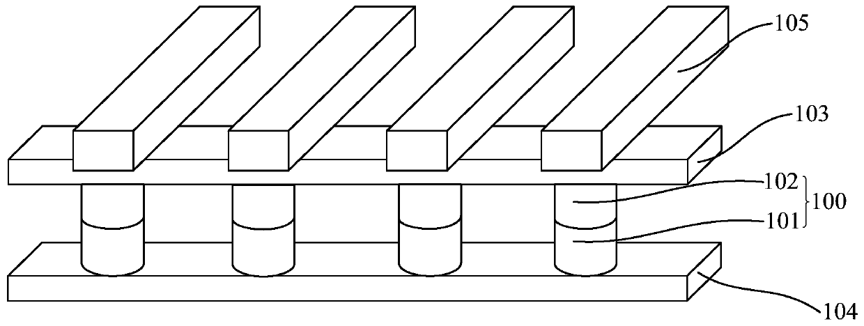
[0085] Such as figure 1 As shown, the present invention provides a storage array structure, and the storage array structure includes:

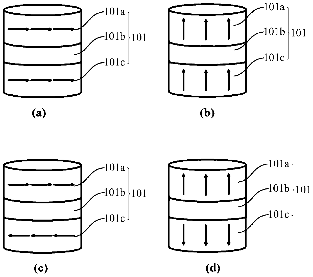
[0086] At least one storage unit 100, the storage unit 100 includes a stacked magnetic storage device 101 and a superconducting device 102, and the magnetic storage device 101 and the superconducting device 102 are arranged in series;

[0087] At least one superconducting upper electrode 103, the superconducting upper electrode 103 is arranged above the storage unit 100, and is electrically connected to the corresponding storage unit 100, when there are at least two superconducting upper electrodes 103, There is no contact between the superconducting upper electrodes 103;

[0088] At least one superconducting lower electrode 104, the superconducting lower electrode 104 is arranged under the storage unit 100, and is electrically connected to the corresponding storage unit 100, when there are at least two superconducting lower electrodes 104, ...

Embodiment 2

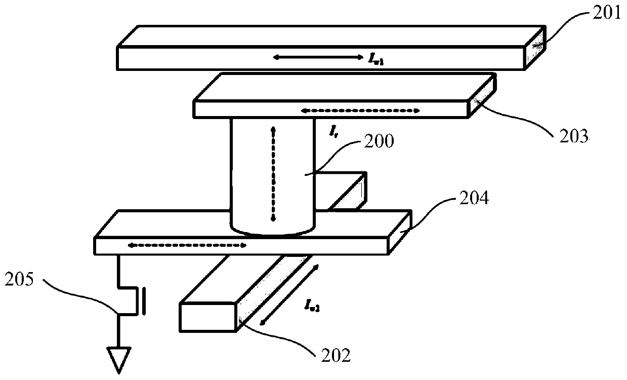
[0128] Such as Figure 8 As shown, the present invention also provides a memory array structure. The difference between the array structure of this embodiment and Embodiment 1 is that the memory array structure further includes at least one superconducting write bit line 106, and the superconducting The guide write bit line 106 is arranged above or below the memory cell 100, and is arranged to cross correspondingly with the corresponding superconducting word line 105, and the superconducting write bit line 106 and the superconducting word line 105. The superconducting write bit line 106 and the superconducting upper electrode 103, the superconducting writing bit line 106 and the superconducting lower electrode 104, and the superconducting writing bit line 106 and the storage unit 100 There is a gap between them, wherein, when there are at least two superconducting write bit lines 106, there is no contact between each of the superconducting write bit lines 106, and other struct...

Embodiment 3

[0136] The present invention also provides a memory, wherein the memory includes the memory array structure described in any one of the above embodiments, wherein the superconducting upper electrode 103 and the superconducting lower electrode 104 serve as the the bit line. In this embodiment, in addition to the device structures and connections described in the above embodiments in the memory, the superconducting device in each of the storage units is arranged in series with the magnetic storage device. The superconducting upper electrode and the superconducting lower electrode are arranged in parallel between the memory cells to form a memory array. The structures and connections of other necessary device structures constituting the memory and the structure of the memory array are well known in the art and will not be repeated here.


PUM


Abstract

The invention provides a memory array structure, a preparation method thereof, a memory, a write-in method and a read-out method. The array structure comprises at least one memory cell which comprisesa superconducting device and a magnetic memory device which are overlapped and connected in series; at least one superconductive upper electrode which is arranged above the memory unit; at least onesuperconductive lower electrode arranged below the memory unit; at least one superconductive word line arranged above the memory unit or below the memory unit, wherein the superconductive word line isarranged close to the superconductive device in the memory unit. According to the invention, the magnetic memory device is organically combined with the superconducting integrated circuit, and the switching effect of the circuit is realized by using a superconducting device, thereby replacing a CMOS logic circuit. The memory array structure can achieve the operation of the memory at low temperature, guarantees that an MRAM achieves high-speed and high-density storage at a low working voltage, achieves the work based on different writing modes, forms an information reading mode suitable for the superconducting logic process, and is simple in structural design and beneficial to reduction of the etching frequency.

Description

technical field [0001] The invention belongs to the technical field of memory, and in particular relates to a memory array structure and a preparation method, a memory, and a writing method and a reading method. Background technique [0002] As a new type of non-volatile storage technology, Magnetic Random Access Memory (MRAM) has high-speed random read and write, high integration, low write power, good fatigue resistance, considerable economic advantages. Therefore, MRAM is widely used in advanced technology fields such as consumer electronics, artificial intelligence, mechanical automation, Internet of Things and big data, and aerospace. [0003] At present, most of the relatively well-developed MRAMs are combined with CMOS logic circuits, and the working temperature range is generally not lower than room temperature. However, there are very few applications of MRAM at low temperatures. How to find magnetic memory cells that maintain excellent electrical properties at ex...

Claims


Application Information

Patent Timeline
Patent Type & Authority Applications(China)
IPC IPC(8): H01L27/11521H01L27/18H01L27/22
Inventor 郎莉莉叶力
Owner SHANGHAI INST OF MICROSYSTEM & INFORMATION TECH CHINESE ACAD OF SCI
Why Eureka
Try Eureka