Semiconductor structure and forming method thereof

A technology of semiconductor and gate structure, which is applied in the field of semiconductor structure and its formation, can solve the problem of serious gate-induced drain leakage current, and achieve the effect of reducing leakage current

Active Publication Date: 2019-06-11
SEMICON MFG INT (SHANGHAI) CORP +1
View PDF3 Cites 0 Cited by
  • Summary
  • Abstract
  • Description
  • Claims
  • Application Information

AI Technical Summary

Problems solved by technology

[0004] However, the gate-induced drain leakage current of

Method used


Image

  • Semiconductor structure and forming method thereof
  • Semiconductor structure and forming method thereof
  • Semiconductor structure and forming method thereof

Examples


Embodiment Construction

[0031] As mentioned in the background, FinFETs have poor performance.

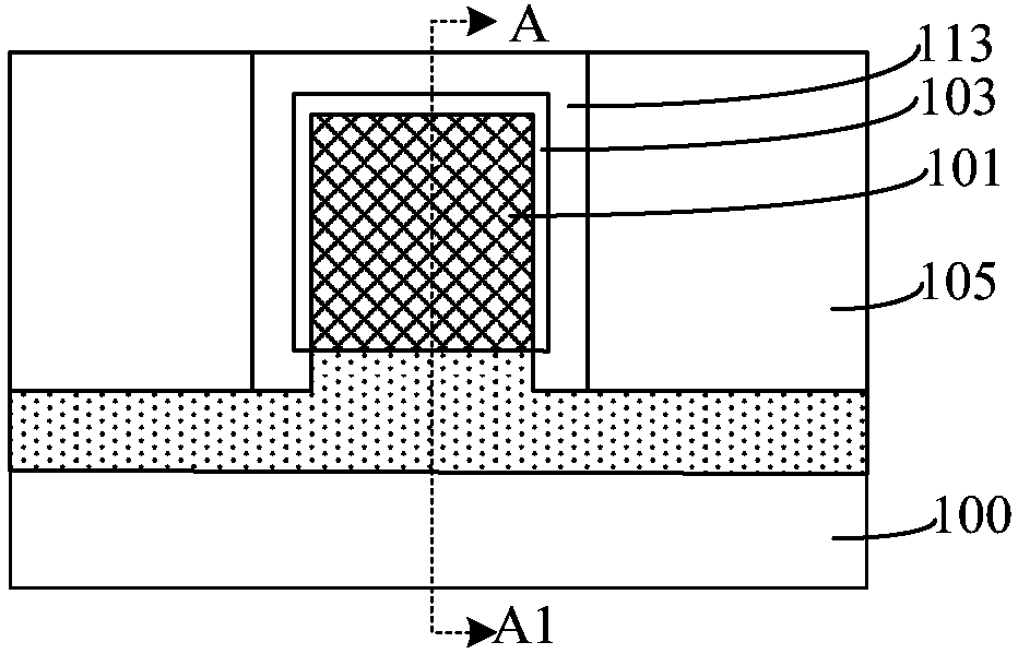
[0032] Figure 1 to Figure 2 A schematic diagram of a semiconductor structure.

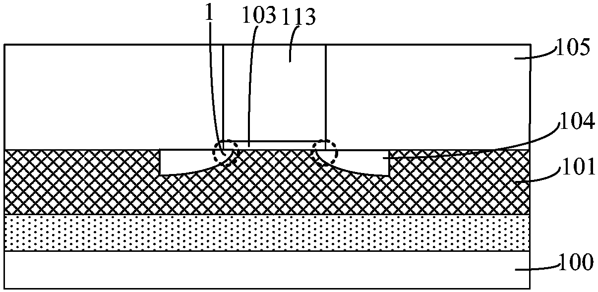
[0033] Please refer to figure 1 and figure 2 , figure 2 yes figure 1 A schematic cross-sectional view along the line A-A1, the substrate 100, the substrate 100 has a fin 101; the gate dielectric layer 103 located on part of the sidewall and top surface of the fin 101 and the gate layer 113 located on the top of the gate dielectric layer 103; The source and drain doped regions 104 respectively located in the fins 101 on both sides of the gate layer 113 (see figure 2 ); the dielectric layer 105 located on the substrate 100 and the source-drain doped region 104 , the top surface of the dielectric layer 105 exposes the top surface of the gate layer 113 .

[0034]In the above method, in order to improve the mobility of carriers in the channel region of the semiconductor device, silicon germanium or germanium is used as th...


PUM

PropertyMeasurementUnit
Thicknessaaaaaaaaaa
Thicknessaaaaaaaaaa
Thicknessaaaaaaaaaa

Abstract

The invention provides a semiconductor structure and a forming method thereof, wherein the method comprises the following steps: providing a substrate, wherein a fin structure is arranged on the substrate, and the material of the fin structure is provided with a first forbidden band width; doping a first doped ion into the top of the fin structure so as to form an improved region, wherein the material of the improved region is provided with a second forbidden band width, and the second forbidden band width is larger than the first forbidden band width; forming a gate structure which spans thefin structure and the improved region, wherein the gate structure covers part of the side wall of the fin structure and the side wall and top surface of the improved region; and forming a source/draindoping region in the improved region on the two sides of the gate structure. According to the method, the gate-induced drain leakage current of the semiconductor device can be reduced.

Description

technical field [0001] The invention relates to the field of semiconductor manufacturing, in particular to a semiconductor structure and a forming method thereof. Background technique [0002] Because there is a large overlapping area between the gate and the drain of a metal oxide semiconductor field effect transistor (Metal Oxide Semiconductor Field Effect Transistor, MOSFET). Taking NMOSFET as an example, when a voltage is applied to the gate, the drain potential in the NMOSFET is more positive than the gate potential, and holes will be generated in the overlapping region due to the effect of the gate voltage, and the holes will pass through The over-depletion region moves into the substrate and forms a substrate current, which is usually a gate-induced drain leakage (Gate-Induced Drain Leakage, GIDL) current. Conversely, when a voltage is applied to the gate, the gate potential in the PMOSFET is more positive than the drain potential, and electrons are generated in the ...

Claims


Application Information

Patent Timeline
IPC IPC(8): H01L21/8238H01L27/092H01L29/06H01L29/10
Inventor 李勇
Owner SEMICON MFG INT (SHANGHAI) CORP
Why Eureka
Try Eureka