LED chip package support and production method thereof

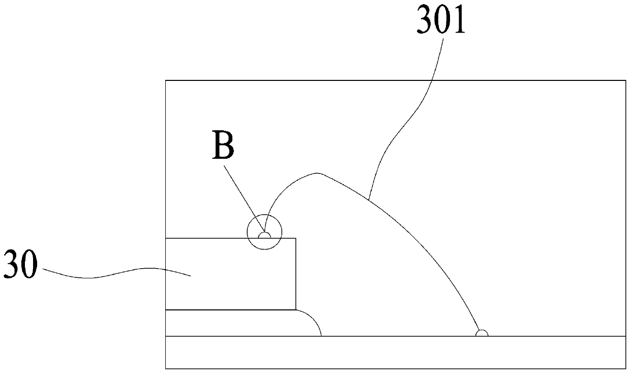
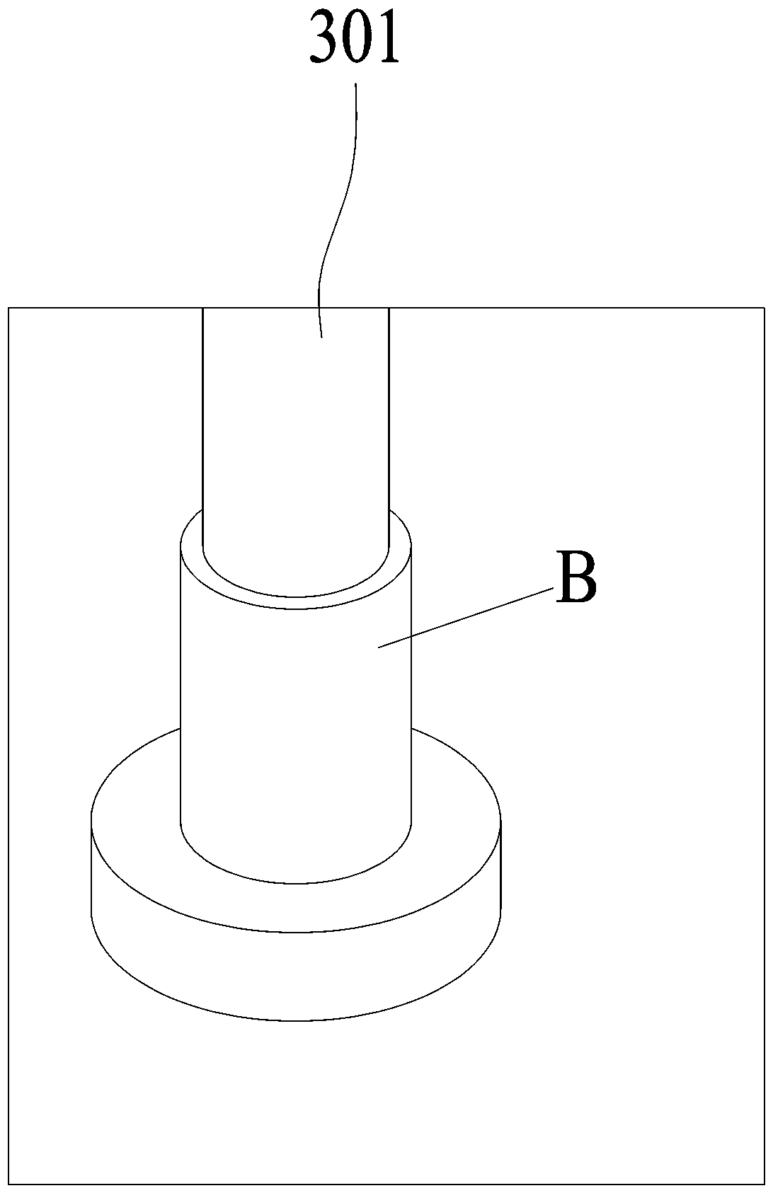
A technology of LED chips and packaging brackets, which is applied in the direction of electrical components, circuits, semiconductor devices, etc., and can solve problems such as the easy break point of the connecting wire 301, the inability to realize the anti-vulcanization performance of SMD LED, and the influence of light extraction efficiency.

Pending Publication Date: 2019-06-14
福建省信达光电科技有限公司
View PDF6 Cites 1 Cited by
  • Summary
  • Abstract
  • Description
  • Claims
  • Application Information

AI Technical Summary

Problems solved by technology

However, the glue 40 with relatively high Shore hardness has relatively large internal stress. Under the impact of thermal expansion and contraction, the connecting wires 301 of the positive and negative electrodes of the LED chip 30 are likely to break. After testing, as shown in FIG. figure 2 and image 3 As shown, the connection point B between the connecting wire 301 and the upper surface of the LED chip 30 is easy to break, and the number of TS rounds of the thermal shock test is less than 100, which affects the light emission.
[0004] In order to solve the problem that the connecting wires 301 of the positive and negative poles of the LED chip 30 are easy to break, in the prior art, a glue 40 with a relatively small Shore hardness is packaged in the reflective cup 10, and phosphor powder is mixed in the glue 40.
However, the glue 40 with less Shore hardness makes the gap between the glue 40 and the reflective cup 10 and the base 20 larger, so that sulfur vapor easily enters the bottom of the reflective cup 10 and reacts with the silver-plated layer to produce black matter. Absorbing luminous flux, affecting light output efficiency
[0005] Therefore, in the prior art, it is impossible to improve both the anti-vulcanization performance of SMD LEDs and the thermal shock resistance of SMD LEDs, and the two cannot be achieved at the same time.

Method used


Image

  • LED chip package support and production method thereof
  • LED chip package support and production method thereof
  • LED chip package support and production method thereof

Examples


Embodiment Construction

[0031] The present invention will be described in detail below with reference to the drawings and specific embodiments.

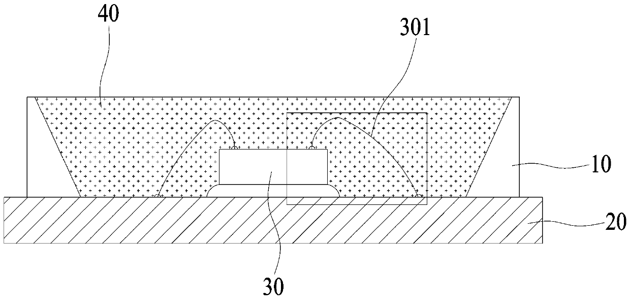
[0032] See Figure 4 and Figure 5 As mentioned, an LED chip packaging support disclosed in the present invention includes a base 1, a reflective cup 2, an LED chip 3, a first silica gel layer 4, and a second silica gel layer 5.

[0033] The reflector cup 2 is arranged on the base 1, the lower surface of the LED chip 3 is mounted on the base 1 and located at the bottom of the reflector cup 2, and the positive and negative poles of the LED chip 3 are respectively connected to the pins by connecting wires 6. This is a conventional structure. I will not repeat them here. The side where the LED chip 3 is attached to the base 1 is the lower surface, and the other side opposite to the lower surface is the upper surface, that is, the side closer to the base 1 is the lower surface, and the side farther from the base 1 is the upper surface .

[0034] The bottom of the r...


PUM


Abstract

The invention discloses an LED chip package support. The LED chip package support comprises a base, a reflection cup, an LED chip, a first silica gel layer and a second silica gel layer, wherein the reflection cup is arranged on the base, a lower surface of the LED chip is surface-mounted onto the base and is arranged at the bottom of the reflection cup, a positive electrode and a negative electrode of the LED chip are connected with a pin by a connection wire, the first silica gel layer is arranged at the bottom of the reflection cup, the second silica gel layer is arranged on the first silica gel layer, the second silica gel layer covers an upper surface of the LED chip, the shore hardness of the first silica gel layer is larger than the shore hardness of the second silica gel layer, andfluorescent powder is mixed in the second silica gel layer. The invention also discloses a production method of the LED chip package support. By the LED chip package support, the vulcanization-prevention performance of an SMD LED is improved, the cold and hot impact resistant performance of the SMD LED is also improved, and meanwhile, the production cost is reduced.

Description

Technical field [0001] The invention relates to the technical field of LED packaging, in particular to an LED chip packaging support and a production method thereof. Background technique [0002] With the development of semiconductor lighting technology, light emitting diodes (LEDs) have been widely used in the field of lighting and display due to their high brightness, low energy consumption, small size, long life and safety and reliability, and are considered to replace The fourth-generation light source for incandescent lamps, fluorescent lamps, and high-pressure gas discharge lamps. There are many types of LEDs, including in-line LEDs, SMD LEDs, piranhas, and high-power LEDs. Among them, SMD LEDs are surface mount light-emitting diodes, which are widely used. [0003] In the prior art, when packaging SMD LEDs, such as figure 1 and figure 2 As shown, the reflector cup 10 is placed on the base 20, the LED chip 30 is mounted on the base 20 and located at the bottom of the refle...

Claims


Application Information

Patent Timeline
Patent Type & Authority Applications(China)
IPC IPC(8): H01L33/48H01L33/50H01L33/62
Inventor 胡康乐吕湘平许辉胜王祖亮楚新
Owner 福建省信达光电科技有限公司
Why Eureka
Try Eureka