Chip cutting method

A cutting method and chip technology, applied in manufacturing tools, plasma welding equipment, laser welding equipment, etc., can solve problems such as chip failure, and achieve the effect of increasing the effective use area and good performance

Active Publication Date: 2021-03-09
INST OF MICROELECTRONICS CHINESE ACAD OF SCI
View PDF6 Cites 0 Cited by
  • Summary
  • Abstract
  • Description
  • Claims
  • Application Information

AI Technical Summary

Problems solved by technology

[0004] The main purpose of this application is to provide a chip cutting method to solve the problem that the laser cutting method in the prior art easily leads to chip failure

Method used


Image

  • Chip cutting method
  • Chip cutting method
  • Chip cutting method

Examples


Embodiment

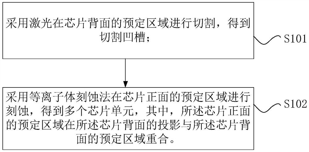
[0042] The chip cutting process includes:

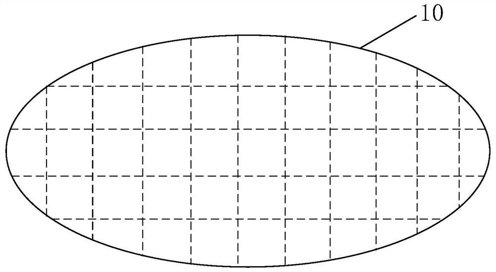
[0043] The chip 10 is turned over so that the back of the chip 10 faces up, that is, the substrate faces up, the substrate of the chip 10 is a single crystal silicon substrate, and a predetermined area on the front of the chip has a mark;

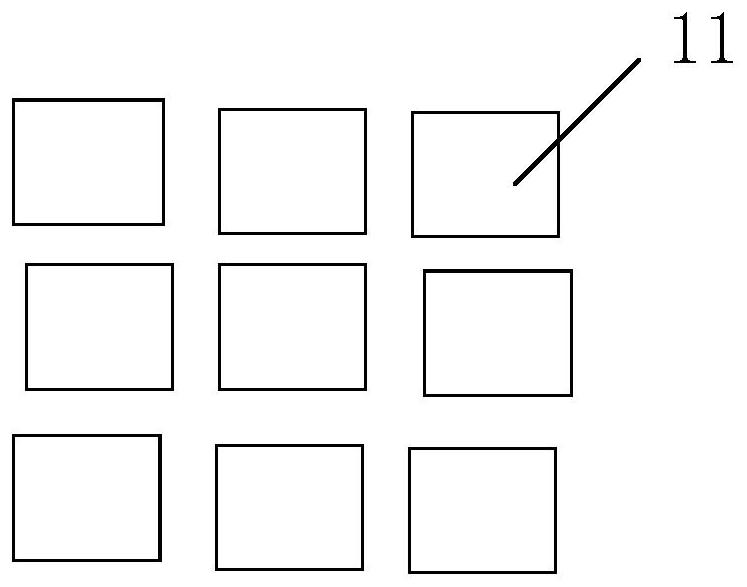
[0044] Laser is used to cut a predetermined area on the back of the chip to obtain a cutting groove, and the cutting groove is 2 / 3 of the thickness of the chip 10, and the obtained figure 2 shown in the structure, figure 2 The dotted lines in indicate where the cutting forms the cutting grooves;

[0045] Turn over the chip 10 again so that the chip is facing up;

[0046] Predetermined light is vertically incident on the above-mentioned chip 10 from the front of the above-mentioned chip, and the predetermined area on the front of the above-mentioned chip is covered with a light-blocking material. The transmittance of light is greater than 60%, and the above-mentioned predetermined light covers...


PUM


Abstract

The application provides a chip cutting method, the cutting method includes: using a laser to cut a predetermined area on the back of the chip to obtain cutting grooves; using a plasma etching method to etch a predetermined area on the front of the chip to obtain multiple A chip unit, wherein the projection of the predetermined area on the front of the chip on the back of the chip coincides with the predetermined area on the back of the chip. In this cutting method, only part of the thickness of the chip is laser cut from the back, and the heat generated by laser cutting is less, which basically does not affect the performance of the chip. Etching increases the effective area of ​​the wafer. This method avoids the problem of chip performance changes or even failure caused by cutting the chip into multiple unit chips by laser cutting, and ensures that each chip formed by cutting The unit performs better.

Description

technical field [0001] The present application relates to the field of semiconductors, and in particular, relates to a chip cutting method. Background technique [0002] After the chip is processed on the wafer, it needs to be separated into units. Nowadays, mechanical cutting and laser cutting are mainly used to realize it. However, these two technologies have certain limitations, which will have a certain impact on the performance or yield of the product. For example, mechanical dicing will inevitably cause damage to the wafer structure, wasting the area of ​​the wafer, and if the damage area is too large, the chip function may fail. Although laser cutting has little damage, the heat generated by the laser may cause chip performance to change or even fail. [0003] The above information disclosed in the Background section is only to enhance the understanding of the background of the technology described herein, therefore, the Background may contain certain information whi...

Claims


Application Information

Patent Timeline
Patent Type & Authority Patents(China)
IPC IPC(8): H01L21/78H01L21/3065B23K10/00B23K26/38
Inventor 王文罗军许静
Owner INST OF MICROELECTRONICS CHINESE ACAD OF SCI
Why Eureka
Try Eureka