A high-speed and low-power level shift circuit

A technology of level shift circuit and low power consumption, which is applied in the direction of logic circuit connection/interface layout, logic circuit coupling/interface using field effect transistors, electronic switches, etc. Increased circuit power consumption and other issues to achieve the effect of increasing the maximum operating frequency, reducing chip power consumption, and reducing turn-off and turn-on time

Active Publication Date: 2022-08-02
58TH RES INST OF CETC
View PDF3 Cites 0 Cited by
  • Summary
  • Abstract
  • Description
  • Claims
  • Application Information

AI Technical Summary

Problems solved by technology

[0005] The purpose of the present invention is to provide a high-speed and low-power level shift circuit to solve the problem that the power consumption of the traditional level shift circuit increases significantly when the high-end drive power tube is turned on, and its turn-off speed is limited by the size of the current source I1. The problem that the working frequency cannot be increased

Method used


Image

  • A high-speed and low-power level shift circuit
  • A high-speed and low-power level shift circuit
  • A high-speed and low-power level shift circuit

Examples


Embodiment 1

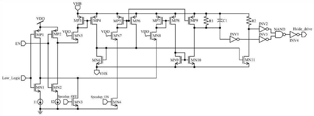
[0025] The present invention provides a high-speed and low-power level shift circuit, the structure of which is as follows: figure 2 shown. The high-speed and low-power level shift circuit includes: resistors R1-R2, capacitors C1, NMOS transistors MN1-MN11, PMOS transistors MP1-MP9, current sources I1-I2, inverters INV1-INV4 and dual-input NAND gates NAND1.

[0026]Specifically, the resistor R1 is connected in parallel with the two ends of the capacitor C1, and one end of the resistor R1 and the capacitor C1 is connected to the floating power supply VHB together, and the other end is connected to the input end of the inverter INV1; the drain ends of the NMOS transistor MN1 and the PMOS transistor MP1 Interconnection, the gate terminal is connected to the low-voltage control logic Low_Logic, the source terminal of the NMOS transistor MN1 is connected to the current source I1; the drain terminals of the NMOS transistor MN2 and the PMOS transistor MP2 are interconnected, and th...


PUM


Abstract

The invention discloses a high-speed and low-power consumption level shift circuit, which belongs to the technical field of integrated circuits. The high-speed and low-power level shift circuit increases the Speedup_OFF and Speedup_ON signals: when Low_Logic becomes high, a narrow pulse of Speedup_OFF is generated to accelerate the shutdown of the high-end driving power tube, and when Low_Logic becomes low, a narrow pulse of Speedup_ON is generated to realize the high-end driving power. The opening of the tube is accelerated. The turn-off and turn-on time of the high-end drive power tube is reduced, the maximum operating frequency of the chip is increased, and the application range of the chip is expanded; when the chip is in a steady state, Speedup_OFF and Speedup_ON are always 0, and the level shift circuit will not introduce additional current. Reduced chip power consumption.

Description

technical field [0001] The present invention relates to the technical field of integrated circuits, in particular to a high-speed and low-power level shift circuit. Background technique [0002] With the rapid development of semiconductor integrated circuit technology, in addition to low-voltage fields such as mobile phones and mobile devices, power integrated circuits have become more and more widely used in high-voltage applications such as high-speed rail and IGBT. Among the many existing intelligent power integrated circuits, the H-bridge power driver chip is a typical representative, and it is a key research direction at home and abroad in recent years. It is suitable for many fields such as DC motor drive, AC motor drive and high-voltage inverter power supply. [0003] In the H-bridge driver chip, N-type LDMOS is selected for both high and low-end power tubes to meet the requirements of low on-resistance. Since the N-type LDMOS needs to ensure that its gate-source vol...

Claims


Application Information

Patent Timeline
Patent Type & Authority Patents(China)
IPC IPC(8): H03K17/04H03K19/0185
Inventor 奚冬杰徐晴昊
Owner 58TH RES INST OF CETC
Why Eureka
Try Eureka