Detection method for electric connection defect of chip

A detection method and defect technology, which is applied in the directions of electronic circuit test, optical test defect/defect, electrical measurement, etc., can solve the problems of electrical connection structure defects, difficulty in meeting the requirements of failure analysis of three-dimensional storage devices, etc., and achieve reduction of superposition phenomenon, The effect of improving detection accuracy and improving detection efficiency

Active Publication Date: 2019-06-28
YANGTZE MEMORY TECH CO LTD
View PDF8 Cites 5 Cited by
  • Summary
  • Abstract
  • Description
  • Claims
  • Application Information

AI Technical Summary

Problems solved by technology

The failure of a three-dimensional memory device may be caused by defects in the active region or by defects in the electrical connection structure
[0005] However, the above detection methods are difficult to meet the requirements of failure analysis of complex electrical connection structures of 3D memory devices. It is expected to further improve the detection method of chip electrical connection defects to improve detection efficiency and accuracy

Method used


Image

  • Detection method for electric connection defect of chip
  • Detection method for electric connection defect of chip
  • Detection method for electric connection defect of chip

Examples


Embodiment Construction

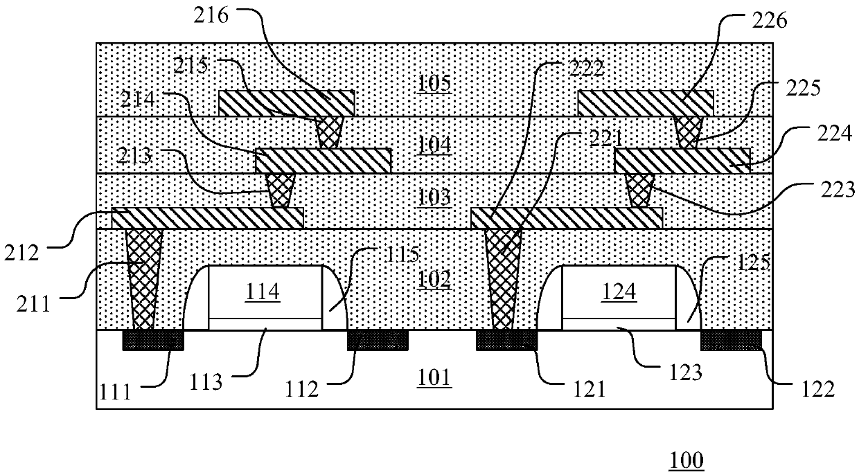
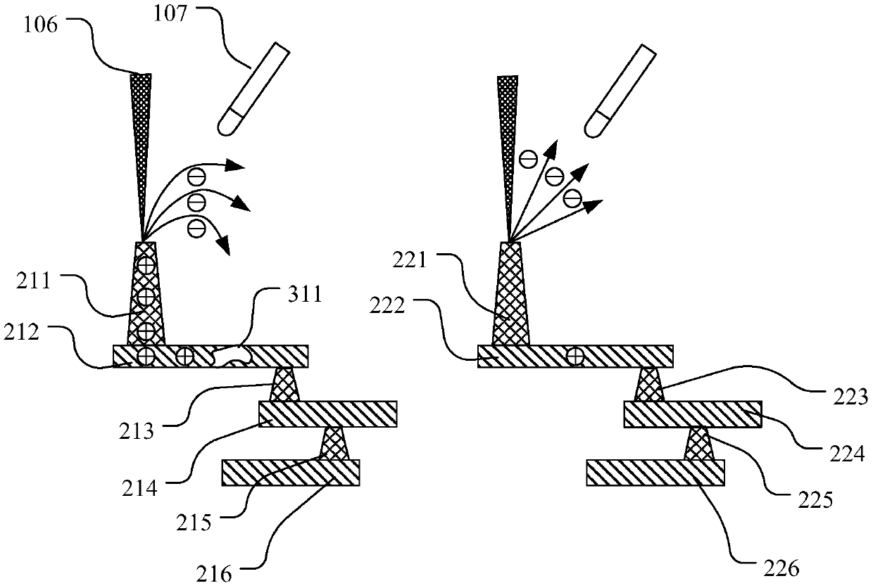
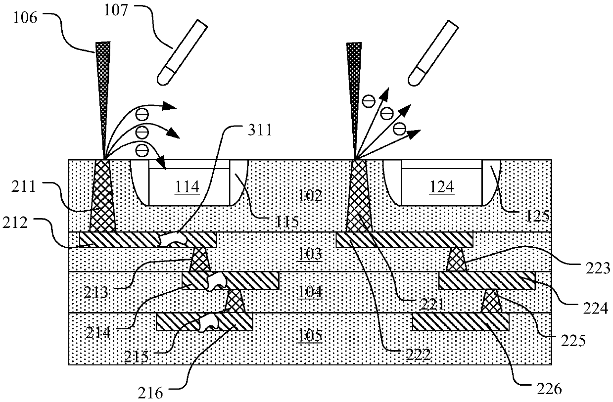
[0021] Hereinafter, the present invention will be described in more detail with reference to the accompanying drawings. In the various figures, identical elements are indicated with similar reference numerals. For the sake of clarity, various parts in the drawings have not been drawn to scale.

[0022] The inventors found that the detection of electrical connection defects using a nano-probe station can only obtain the detection results of the contact position, and the spatial resolution of the detection is limited by the size of the probe. For a chip with a large area, multi-point detection is required, resulting in a long detection time. too long. Therefore, it is difficult for nanoprobe stations to meet the large-area inspection requirements of three-dimensional memory devices. Scanning electron microscopy can be used to obtain the topography of the field of view, and the defect position can be found by observing the topography image of the chip layer by layer. The spati...


PUM


Abstract

The invention discloses a detection method for an electric connection defect of a chip. The method comprises that a substrate is removed to expose the end portion of a conductive channel in the lowermost layer connected to an active region on a substrate; a first mode of an electron scanning microscope is used to obtain morphology images of multiple layers of conductive channels from the lowermostone; a second mode of the electron scanning microscope is used to obtain morphology images of interconnection lines of the layers from the lowermost layer; in the morphology images of multiple layersof conductive channels, defect positioning information of the interconnection line in the subsequent layer is obtained according to the contrast of the end portions of the different conductive channels; and in the morphology images of the interconnection lines of the layers, a defect position is discovered according to the defect positioning information. The work voltage of the first mode is lower than that of the second mode. The method can be used to locate the defect position rapidly.

Description

technical field [0001] The invention relates to the technical field of semiconductor manufacturing, and more specifically, to a detection method for chip electrical connection defects. Background technique [0002] The improvement of the storage density of the memory device is closely related to the progress of the semiconductor manufacturing process. As the critical dimension (CD for short) of the pattern feature becomes smaller and smaller, the storage density of the memory device becomes higher and higher. A three-dimensional memory device includes a plurality of memory cells stacked along the vertical direction, which can double the integration level on a wafer per unit area and reduce the cost. [0003] There are a large number of electrical connection structures inside the three-dimensional memory device, which are used to provide conductive paths for the bit line, word line, selection line and source line of the three-dimensional memory device, such as longitudinally...

Claims


Application Information

Patent Timeline
Patent Type & Authority Applications(China)
IPC IPC(8): G01R31/28G01R31/04G01N21/88G01N21/01
Inventor 安健鑫袁刚官绪冬吴继君
Owner YANGTZE MEMORY TECH CO LTD
Why Eureka
Try Eureka