

Nano-column array heterojunction and preparation method thereof
A nanocolumn array and heterojunction technology, which is applied in semiconductor/solid-state device manufacturing, electrical components, circuits, etc., can solve the problem of lack of one-dimensional nanocolumn array heterojunction nanocolumn array heterojunction, and achieve experimental methods The effect of simplicity, less gaps, and obvious array structure
- Summary
- Abstract
- Description
- Claims
- Application Information
AI Technical Summary
Problems solved by technology
Method used
Image


Examples
Embodiment 1
[0029] Weigh Bi respectively 2 Te 3 with Sb 2 Te 3 The powder with a molar ratio of 1:1 was placed in two different evaporation sources of a multi-source high vacuum thermal evaporation coating machine, the substrate was made of quartz glass, and the distance between the two evaporation sources and the substrate was adjusted to be 5cm. First stage, vacuum down to 9×10 -5 Pa, increase substrate temperature to 250°C, then increase Bi 2 Te 3 Evaporation source temperature to 520°C, vapor deposition for 20min; the second stage, close the Bi 2 Te 3 Evaporation source, open Sb 2 Te 3 Evaporate the source and heat up to 550°C, adjust the pressure to 7×10 - 5 Pa, vapor deposition for 20min. After evaporation, the temperature was lowered and the product was collected.
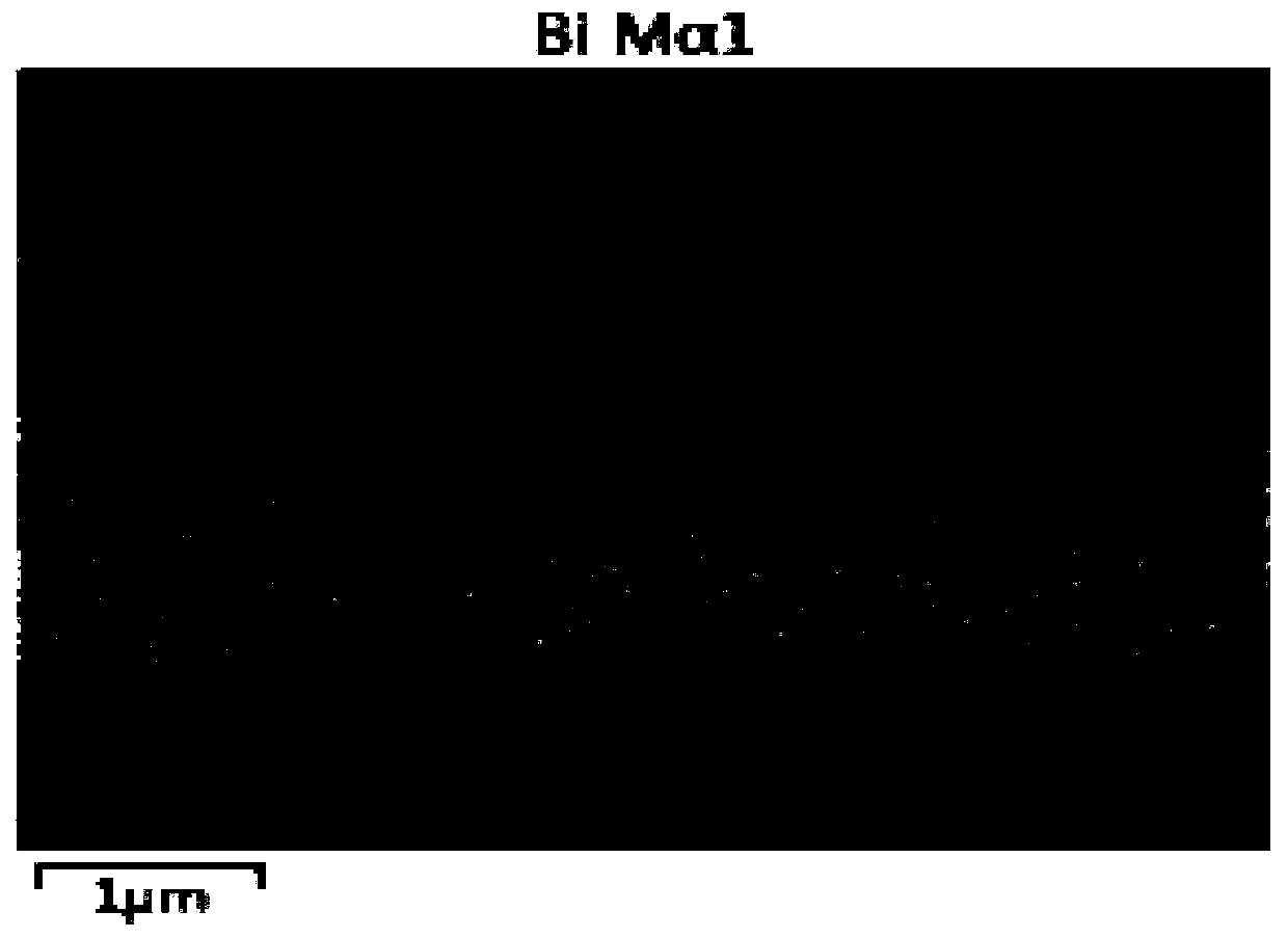
[0030] Scanning electron microscopy was performed on the heterojunction of the nanopillar array prepared in Example 1 of the present invention. like figure 1 and figure 2 as shown, figure 1 It is a surf...
Embodiment 2
[0033] Weigh Bi respectively 2 Te 3 with Sb 2 Te 3 The powder with a molar ratio of 1:1 was placed in two different evaporation sources of a multi-source high vacuum thermal evaporation coating machine, the substrate was made of quartz glass, and the distance between the two evaporation sources and the substrate was adjusted to be 5cm. First stage, vacuum down to 9×10 -5 Pa, increase substrate temperature to 250°C, then increase Bi 2 Te 3Evaporation source temperature to 530°C, evaporation for 15min; the second stage, close the Bi 2 Te 3 Evaporation source, open Sb 2 Te 3 Evaporate the source and heat up to 550°C, adjust the pressure to 7×10 - 5 Pa, vapor deposition for 15min. After evaporation, the temperature was lowered and the product was collected.
Embodiment 3
[0035] Weigh Bi respectively 2 Te 3 with Sb 2 Te 3 The powder with a molar ratio of 1:1 was placed in two different evaporation sources of a multi-source high vacuum thermal evaporation coating machine, the substrate was made of quartz glass, and the distance between the two evaporation sources and the substrate was adjusted to be 5cm. First stage, vacuum down to 9×10 -5 Pa, increase substrate temperature to 230°C, then increase Bi 2 Te 3 Evaporation source temperature to 500°C, evaporation for 20min; the second stage, close the Bi 2 Te 3 Evaporation source, open Sb 2 Te 3 Evaporate the source and heat up to 530°C, adjust the pressure to 7×10 - 5 Pa, vapor deposition for 20min. After evaporation, the temperature was lowered and the product was collected.
PUM
 Abstract
Description
Claims
Application Information