Circuit substrate, manufacturing method thereof, display substrate and splicing display device

A technology for circuit substrates and manufacturing methods, applied in circuits, electrical components, electrical solid devices, etc., can solve the problems of poor processing performance of glass substrates, easy wear and tear of conductive connections, and reduced product reliability, and achieves water and oxygen corrosion resistance. Good performance, improved service life and reliability, and reduced power consumption

Active Publication Date: 2019-06-28
BOE TECH GRP CO LTD +1
View PDF8 Cites 30 Cited by
  • Summary
  • Abstract
  • Description
  • Claims
  • Application Information

AI Technical Summary

Problems solved by technology

[0004] The object of the present invention is to provide a circuit substrate and its manufacturing method, a display substrate, and a splicing display device, which are used to solve the problem of poor processing performance of the glass substrate when the glass substrate is used to manufacture Micro LED and mini LED backlight substrates or display substrates. When high-density and high-precision drilling is performed, the glass substrate is prone to fragility and cracking; and when Micro LED and mini LED backlight substrates or display substrates are used for splicing, the conductive connection parts on the side of the substrate are easy to wear, resulting in There is a problem of lowering product reliability

Method used


Image

  • Circuit substrate, manufacturing method thereof, display substrate and splicing display device
  • Circuit substrate, manufacturing method thereof, display substrate and splicing display device
  • Circuit substrate, manufacturing method thereof, display substrate and splicing display device

Examples


Embodiment Construction

[0062] In order to further illustrate the circuit substrate, the manufacturing method thereof, the display substrate, and the spliced ​​display device provided by the embodiments of the present invention, a detailed description will be given below in conjunction with the accompanying drawings.

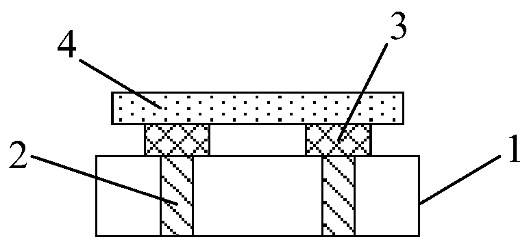
[0063] Based on the problems in the background technology, the inventors of the present invention have found through research that when using a glass substrate, such as figure 1 and figure 2 As shown, it can be considered to form via holes on the glass substrate 1 first, then form Cu pillars 2 by electroforming in the via holes, and form pads 3 on the Cu pillars 2, and finally micro light emitting diodes 4, such as Micro LED Or the mini LED is mounted on the pad 3. Although this method can ensure that the formed via hole has good conductivity when the glass substrate is used, there are still two main problems in this method that are difficult to overcome in practical applications. On...


PUM


Abstract

The invention discloses a circuit substrate, a manufacturing method thereof, a display substrate and a splicing display device, relates to the technical field of display, and aims to solve the problems that when a glass substrate is adopted for manufacturing Micro LED and mini LED backlight substrates or display substrates, the processability of the glass substrate is poor, and the glass substrateis prone to damage during high-precision punching; and when the Micro LED and mini LED backlight substrates or the display substrates are used for splicing, the conductive connecting parts on the side surfaces of the substrates are easy to wear, resulting in the reduction of the reliability of the product. The circuit substrate comprises a substrate provided with a plurality of grooves in the surface; a driving circuit which is arranged on the substrate base plate and comprises a signal line located on the top surface of the substrate, a signal line lead located on the bottom surface of the substrate and a conductive connecting part, wherein the conductive connecting part is connected with the corresponding signal line lead and the corresponding signal line lead respectively. The circuitsubstrate provided by the invention is used for manufacturing a backboard or a splicing display screen.

Description

technical field [0001] The invention relates to the field of display technology, in particular to a circuit substrate and a manufacturing method thereof, a display substrate, and a spliced ​​display device. Background technique [0002] With the continuous development of display technology, new display technologies such as Micro LED (English: Light-Emitting Diode, LED for short) and mini LED are more and more widely used in the field of backlight. [0003] At present, both Micro LED and mini LED are integrated on the printed circuit board (English: Printed Circuit Board, referred to as: PCB) whether they are used for the backlight of the liquid crystal display device or the backlight of the large-size TV, and adopt passive The driving method realizes light emission. Although this method can realize the normal backlight function, it still has certain defects in terms of dynamic local backlight brightness adjustment, reliability, and power consumption. In order to solve the a...

Claims


Application Information

Patent Timeline
Patent Type & Authority Applications(China)
IPC IPC(8): H01L23/498H01L21/48H01L27/15G02F1/13357
CPCH01L21/486H01L23/49805H01L25/0753H01L27/1218H01L27/124H01L23/13H01L23/5386H01L21/0273H01L25/167H01L27/1262H01L27/1288
Inventor 曲连杰齐永莲赵合彬邱云徐晓玲杨瑞智石广东徐诗雨张珊
Owner BOE TECH GRP CO LTD
Why Eureka
Try Eureka