
SERS chip and preparation method and application thereof

A chip and substrate technology, which is applied in the field of SERS chips and their preparation, can solve the problems of research without the application of black phosphorus materials, and achieve the effects of low price, simple operation and mild conditions.

Inactive Publication Date: 2019-07-05
SHENZHEN INST OF ADVANCED TECH +1
View PDF6 Cites 3 Cited by
  • Summary
  • Abstract
  • Description
  • Claims
  • Application Information

AI Technical Summary

Problems solved by technology

There is no research on the application of black phosphorus materials in SERS chips

Method used

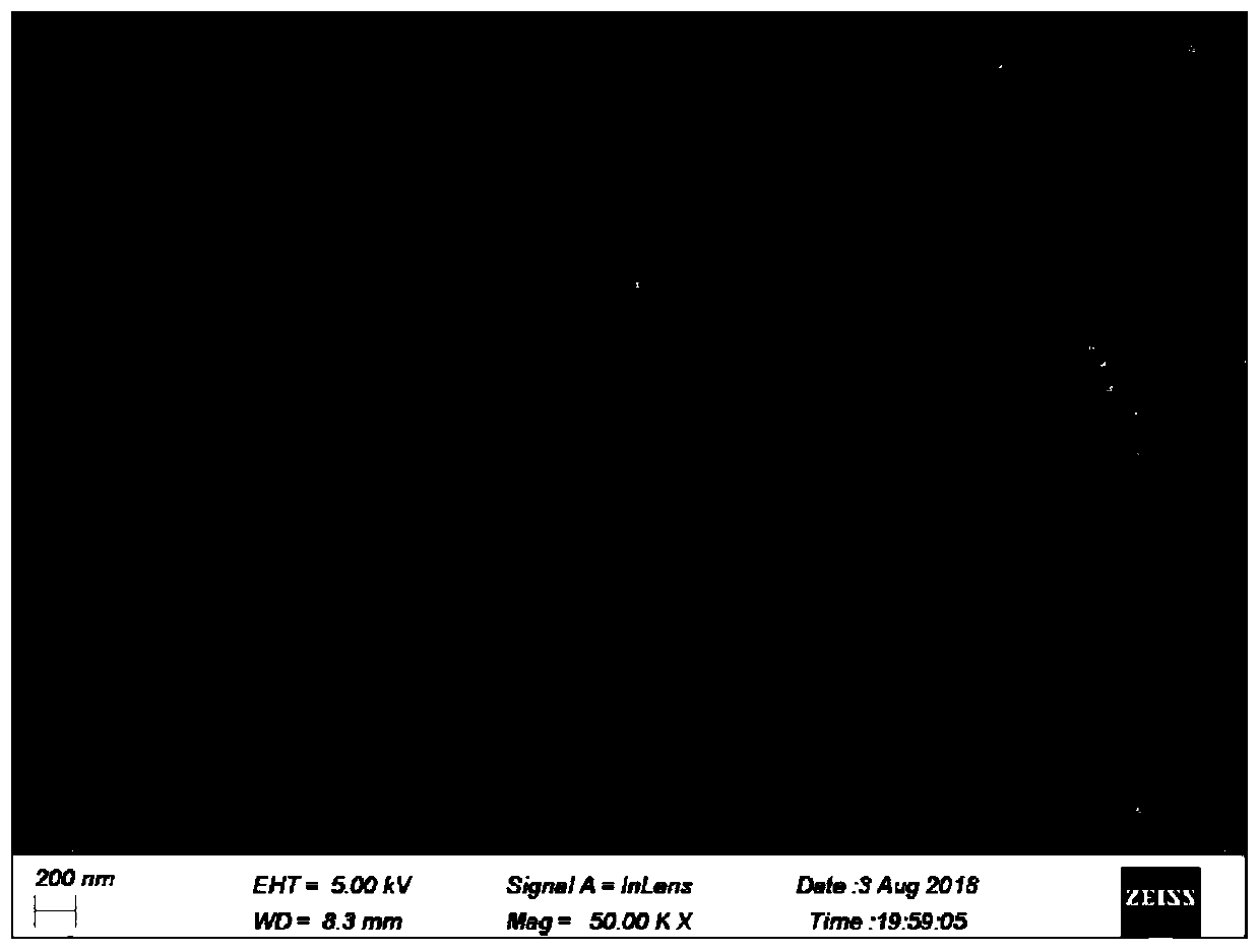
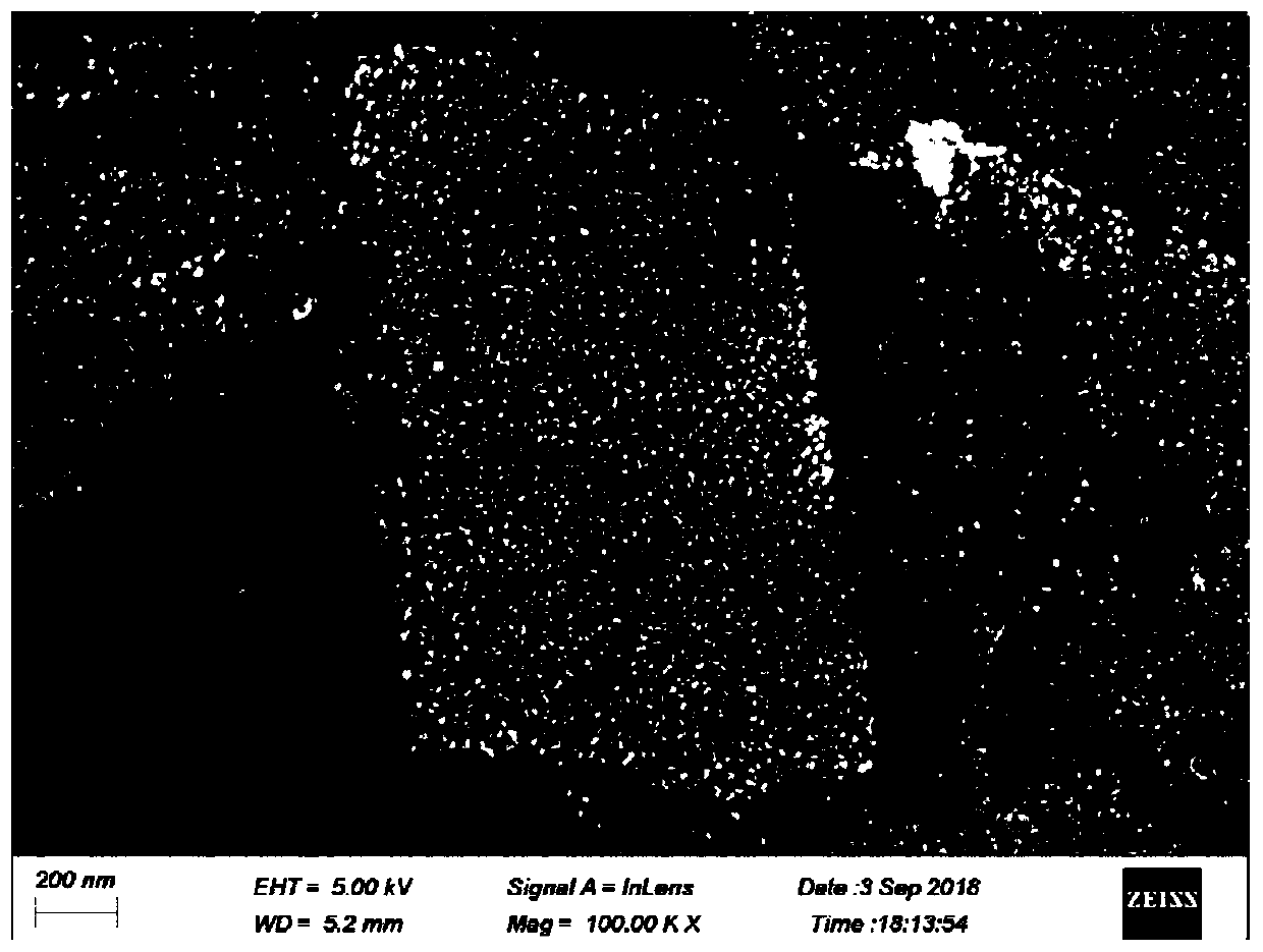
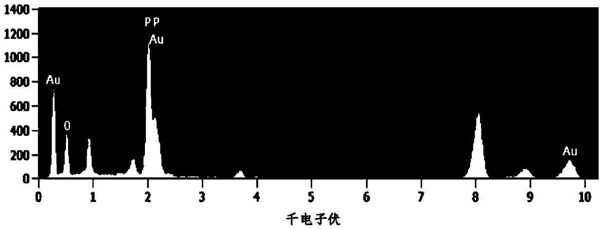

Image

  • SERS chip and preparation method and application thereof
  • SERS chip and preparation method and application thereof
  • SERS chip and preparation method and application thereof

Examples


Embodiment 1

[0028] This embodiment provides a SERS chip, comprising a substrate, a black phosphorus layer covered on the substrate, and silver nanoparticles distributed on the surface of the black phosphorus layer, prepared according to the following steps:

[0029] (1) Preparation of two-dimensional black phosphorus nanosheet solution by electrochemical stripping: using an electrochemical workstation, in an electrolytic cell, use black phosphorus crystals as cathodes, platinum electrodes as anodes, and 0.05mol / L tetrabutylphosphorus bromide The dimethylformamide solution is the electrolyte, and the dimethylformamide solution of the two-dimensional nanosheets is obtained under the action of an electric field of 20V for 20 minutes, and then centrifuged and washed in ethanol to obtain the two-dimensional black phosphorus nanosheet solution.

[0030] After centrifuging and concentrating the electrochemically exfoliated two-dimensional black phosphorus nanosheets solution 5 times, 10 μL was ad...

Embodiment 2

[0034] This embodiment provides a SERS chip, comprising a substrate, a black phosphorus layer covered on the substrate, and gold nanoparticles distributed on the surface of the black phosphorus layer, prepared according to the following steps:

[0035] (1) Preparation of two-dimensional black phosphorus nanosheet solution by electrochemical stripping: using an electrochemical workstation, in an electrolytic cell, use black phosphorus crystals as cathodes, platinum electrodes as anodes, and 0.05mol / L tetrabutylphosphorus bromide The dimethylformamide solution is the electrolyte, and the dimethylformamide solution of the two-dimensional nanosheets is obtained under the action of an electric field of 20V for 20 minutes, and then centrifuged and washed in ethanol to obtain the two-dimensional black phosphorus nanosheet solution.

[0036] After the electrochemically exfoliated two-dimensional black phosphorus nanosheet solution was concentrated by centrifugation at 2000 rpm, 10 μL w...


PUM

PropertyMeasurementUnit
thicknessaaaaaaaaaa
thicknessaaaaaaaaaa
particle diameteraaaaaaaaaa

Abstract

The invention discloses an SERS chip and a preparation method and application thereof. The SERS chip comprises a substrate, a black phosphorus layer covering the substrate, and noble metal nanoparticles distributed on the surface of the black phosphorus layer. The noble metal nanoparticles on the SERS chip prepared by the invention are closely arranged to form a 'hot spot' region for SERS detection. The SERS chip exhibits an outstanding application potential in high-performance SERS detection, is suitable for surface enhanced Raman scattering detection as a substrate, and has a broad application prospect in food analysis, environmental analysis, drug analysis and other fields.

Description

technical field [0001] The invention relates to a chip, in particular to a SERS chip and its preparation method and application. Background technique [0002] The surface-enhanced Raman scattering (Surface-Enhanced Raman Scattering, SERS) effect can enhance the molecular Raman signal by a million times or even higher. It is a non-destructive, label-free, and highly sensitive detection and analysis method. Detection of biological assay samples. The high-performance SERS chip is the key to the sensitivity of SERS detection, and the high-performance SERS chip often relies on the SERS "hot spot" on its surface: it is mainly caused by surface plasmon resonance in the gap between adjacent noble metal nanoparticles as the substrate. A "point" with a very strong localized electric field created by the location. When the detection molecule is adsorbed at the "hot spot" position, its Raman signal will be greatly enhanced, resulting in better SERS performance. [0003] Black Phospho...

Claims


Application Information

Patent Timeline
Patent Type & Authority Applications(China)
IPC IPC(8): G01N21/65
CPCG01N21/658
Inventor 李鹏辉陈婉玲但琨喻学锋胡祥娜禹绍周王瑞
Owner SHENZHEN INST OF ADVANCED TECH
Learn More