Wafer surface defect mode detection and analysis method

A defect mode and analysis method technology, which is applied in character and pattern recognition, semiconductor/solid-state device testing/measurement, instruments, etc., can solve the problem of manual extraction of wafer defect mode diagrams, inability to analyze the cause of defect modes, and low classification accuracy, etc. problem, achieve the effect of reducing labor cost, high labor intensity and improving efficiency

Active Publication Date: 2019-07-05
BEIJING UNIV OF TECH
View PDF11 Cites 22 Cited by
  • Summary
  • Abstract
  • Description
  • Claims
  • Application Information

AI Technical Summary

Problems solved by technology

However, these methods all have complex feature engineering, which requires manual extraction of wafer defect pattern features, and the classification accuracy is low.
At the same time, the above methods are limited to the classification of wafer defect modes, and in each defect mode, the fundamental defects of the wafer are different, and the above methods cannot analyze the cause of defect modes

Method used


Image

  • Wafer surface defect mode detection and analysis method
  • Wafer surface defect mode detection and analysis method
  • Wafer surface defect mode detection and analysis method

Examples


Embodiment Construction

[0045] The method will be described in detail below in conjunction with the accompanying drawings and examples.

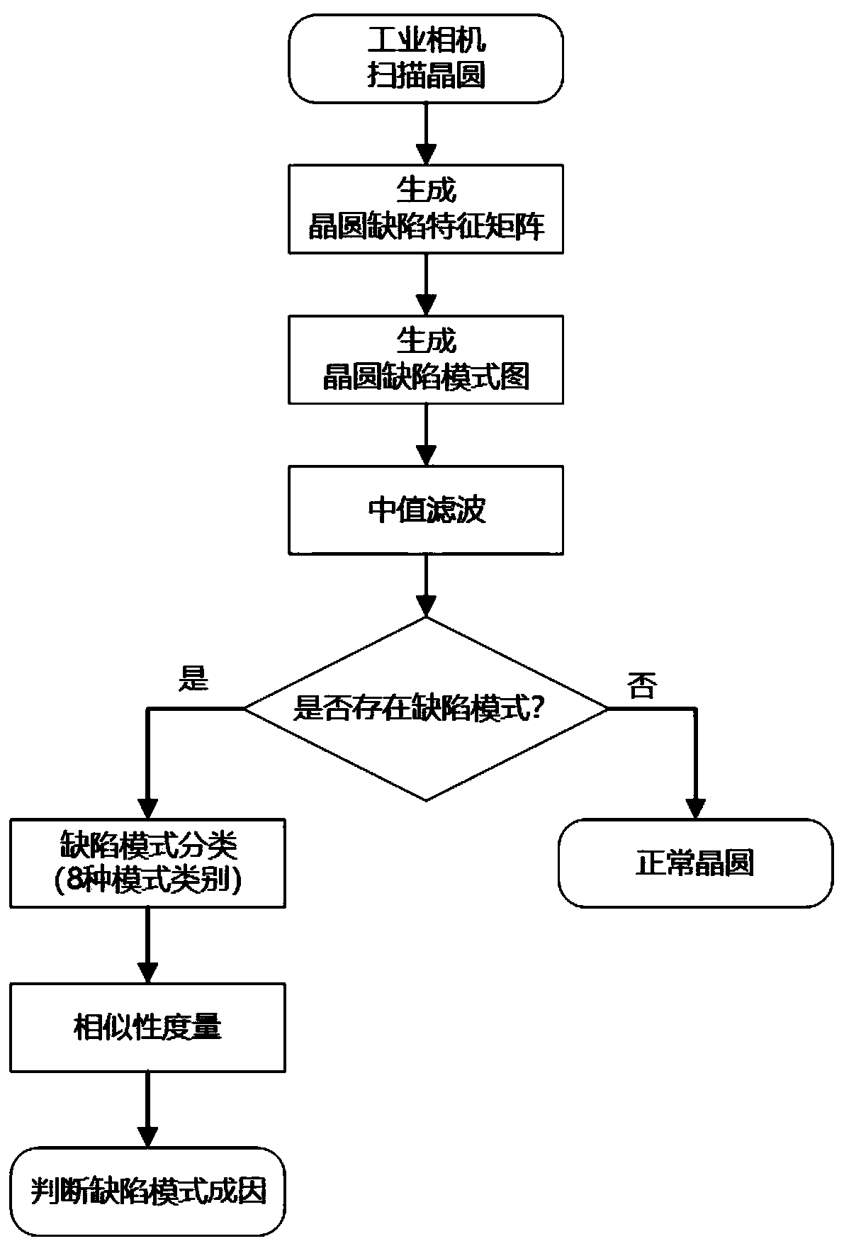
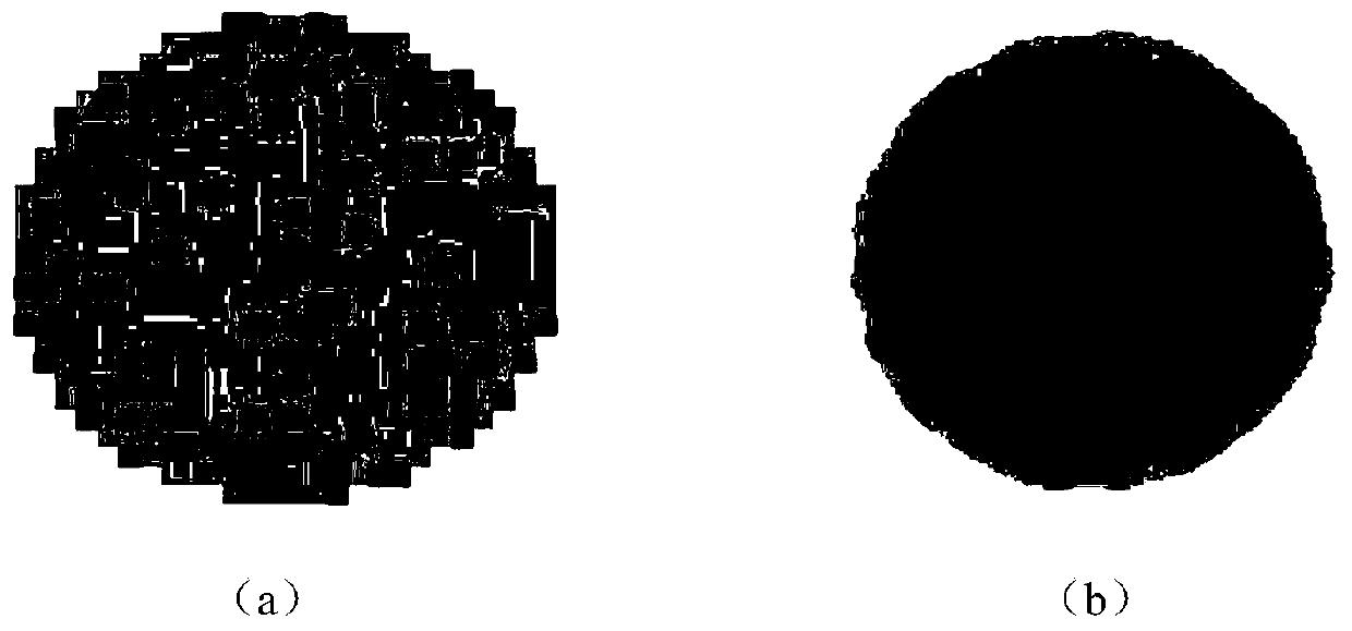
[0046] figure 1 is the flow chart of wafer surface defect pattern detection and analysis method. Firstly, the crystal grains on the wafer are scanned to generate a wafer defect pattern map, which is input into the trained wafer defect pattern detection model after image preprocessing. If there is a defect mode, it is a normal wafer, and the inspection process is exited; if there is a defect mode, it is input into the classification model to determine the specific defect mode type. Finally, according to the proposed similarity measurement algorithm, the most similar sample to the sample to be tested is found in the database, and the root cause of the defect of the sample to be tested is inferred by analyzing the cause of the defect pattern of the similar sample. Specific steps are as follows:

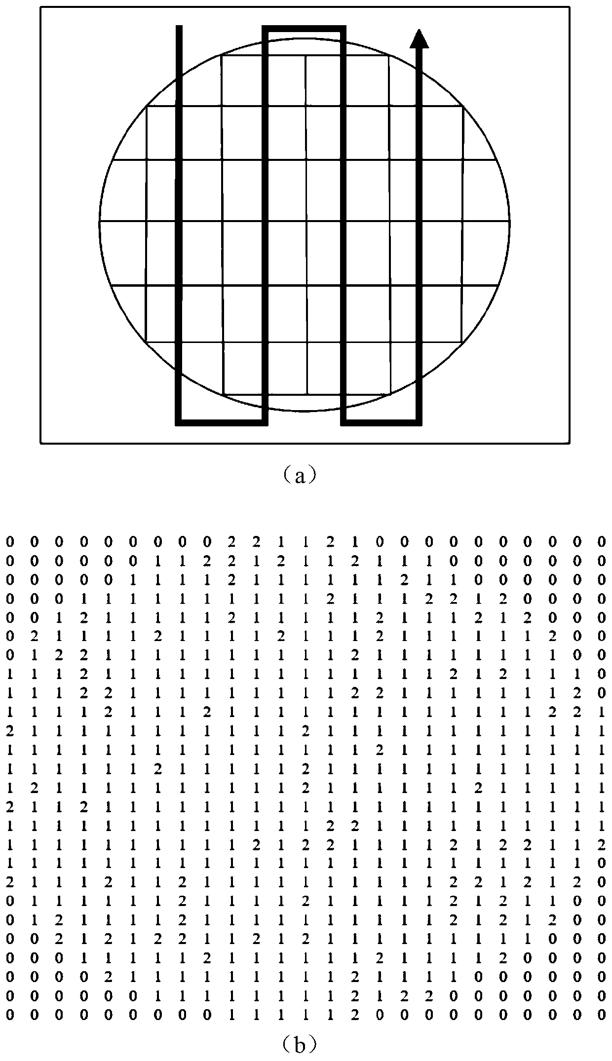
[0047] 1. Acquisition of Wafer Image

[0048] The image acquisition e...


PUM


Abstract

The invention provides a wafer surface defect mode detection and analysis method which can detect surface defects of crystal grains and judge distribution modes and defect mode causes of the defectivecrystal grains. The invention belongs to the field of defect detection in the wafer production and manufacturing process, and aims to solve the problems of high manual labor intensity, low detectionefficiency and the like in the existing defect detection method. The specific process comprises the following steps: acquiring a crystal grain image, and generating a wafer defect mode diagram througha machine vision method; constructing and training a wafer defect mode detection model and a classification model, the detection model being used for determining whether the wafer has a defect mode,and the classification model being used for determining a specific defect mode type; and finally, retrieving the marked sample most similar to the to-be-detected sample in a database according to a similarity measurement algorithm, and inferring the defect mode cause of the to-be-detected sample by analyzing the defect mode cause of the known sample.

Description

[0001] Technical field: [0002] The invention belongs to the field of defect detection in the wafer manufacturing process. Specifically, it relates to a method for detecting defects on the surface of a wafer by using a machine vision method, judging the type of the defect mode, and analyzing the cause of the defect mode. Background technique [0003] Integrated circuits are the basis and source of power for the rapid development of today's information technology industry, and have been highly penetrated and integrated into every field of national economy and social development. One of the signs. In recent years, my country has continuously introduced industrial policies and guidelines to promote and guide the development of the integrated circuit industry. The production and manufacturing of integrated circuits has a very complicated process. Among them, wafers are the main material for manufacturing chips, and their surface defects are the main obstacle affecting product y...

Claims


Application Information

Patent Timeline
Patent Type & Authority Applications(China)
IPC IPC(8): G06K9/00G06K9/62H01L21/66
CPCH01L22/10G06V20/698G06F18/214
Inventor 于乃功徐乔魏雅乾王宏陆王林
Owner BEIJING UNIV OF TECH
Why Eureka
Try Eureka