
A general experimental device and experimental method for power electronic circuits

A technology for power electronic circuits and experimental devices, applied in the field of power electronics, can solve the problems of time-consuming and labor-consuming, large component consumption, etc., and achieve the effects of saving installation time, improving utilization, and convenient use.

Active Publication Date: 2021-04-02
西安华谱电力设备制造有限公司
View PDF9 Cites 0 Cited by
  • Summary
  • Abstract
  • Description
  • Claims
  • Application Information

AI Technical Summary

Problems solved by technology

[0004] The purpose of the present invention is to provide a general experimental device for power electronic circuits, which solves the problems that the existing circuit experiments usually need to repeatedly build circuits, resulting in high cost of components and time-consuming and labor-intensive problems.

Method used


Image

  • A general experimental device and experimental method for power electronic circuits
  • A general experimental device and experimental method for power electronic circuits
  • A general experimental device and experimental method for power electronic circuits

Examples


Embodiment 1

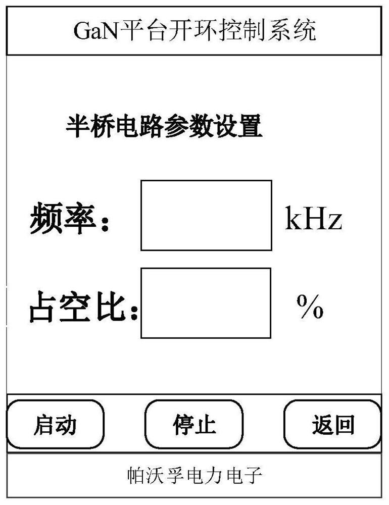
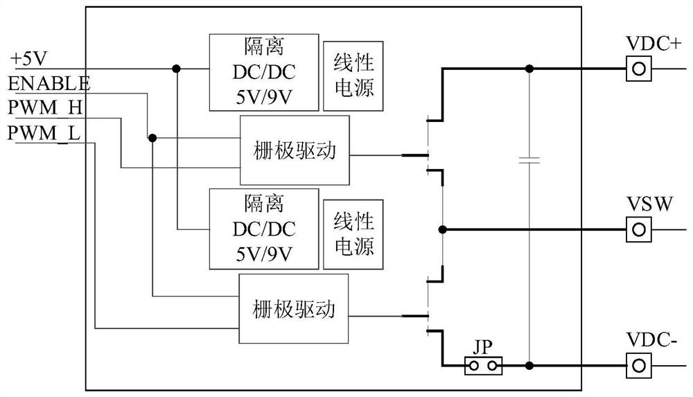
[0055] implement a BUCK chopper circuit such as Figure 4 As shown, a half-bridge sub-board cooperates with a half-bridge mother board to build a circuit. The open-loop controller is set to work in the half-bridge circuit mode. The frequency and duty cycle of the gate control signal are set as required. One output port is connected to the BNC interface of the half-bridge motherboard, the port CON-II is connected to the positive pole of the DC power supply, the port CON-VI is connected to the negative pole of the DC power supply, the inductor is connected between the port VSW and the port CON-V, and the port CON-IV and the port CON- Connect the load between VII, connect one end of the first GaN MOS transistor of the half bridge sub-board to the port CON-II, connect one end of the second GaN MOS transistor to the port CON-VI, and connect the two ends of the GaN MOS transistor to the port CON-II A capacitor is connected in parallel between the first GaN MOS tube and the other end...

Embodiment 2

[0057] Implement full-bridge LLC test circuits such as Figure 5 As shown, two half-bridge sub-boards cooperate with one H-bridge motherboard to build a circuit. The open-loop controller selects the full-bridge circuit working mode, and sets the frequency and duty cycle of the gate control signal according to the needs. The first step of the open-loop controller One output terminal and the third output port are connected to the two BNC interfaces of the H-bridge motherboard, the port CON-III is connected to the positive pole of the power supply, the port CON-IV is connected to the negative pole of the power supply, and the inductor is connected between the port CON-I and the port CON-II. Capacitor, the primary side of the transformer, the secondary side of the transformer is connected to the load, one end of the first GaN MOS tube of a half-bridge sub-board is connected to the port CON-III, the other end is connected to one end of the second GaN MOS tube and connected to On th...

Embodiment 3

[0059] Implement phase-shifted full-bridge test circuits such as Image 6 As shown, the open-loop controller selects the working mode of the full-bridge circuit, and sets the frequency and duty cycle of the gate control signal according to the needs. The first output port and the third output port of the open-loop controller are connected to the two ports of the H-bridge motherboard. BNC interface, the port CON-III is connected to the positive pole of the power supply, the port CON-IV is connected to the negative pole of the power supply, the inductor is connected between the port CON-I and the port CON-II, the primary side of the transformer is connected to the load, and a half-bridge daughter board One end of the first GaN MOS tube is connected to port CON-III, the other end is connected to one end of the second GaN MOS tube and connected to port CON-II, and the other end of the second GaN MOS tube is connected to On port CON-IV, one end of the first GaN MOS transistor of th...


PUM


Abstract

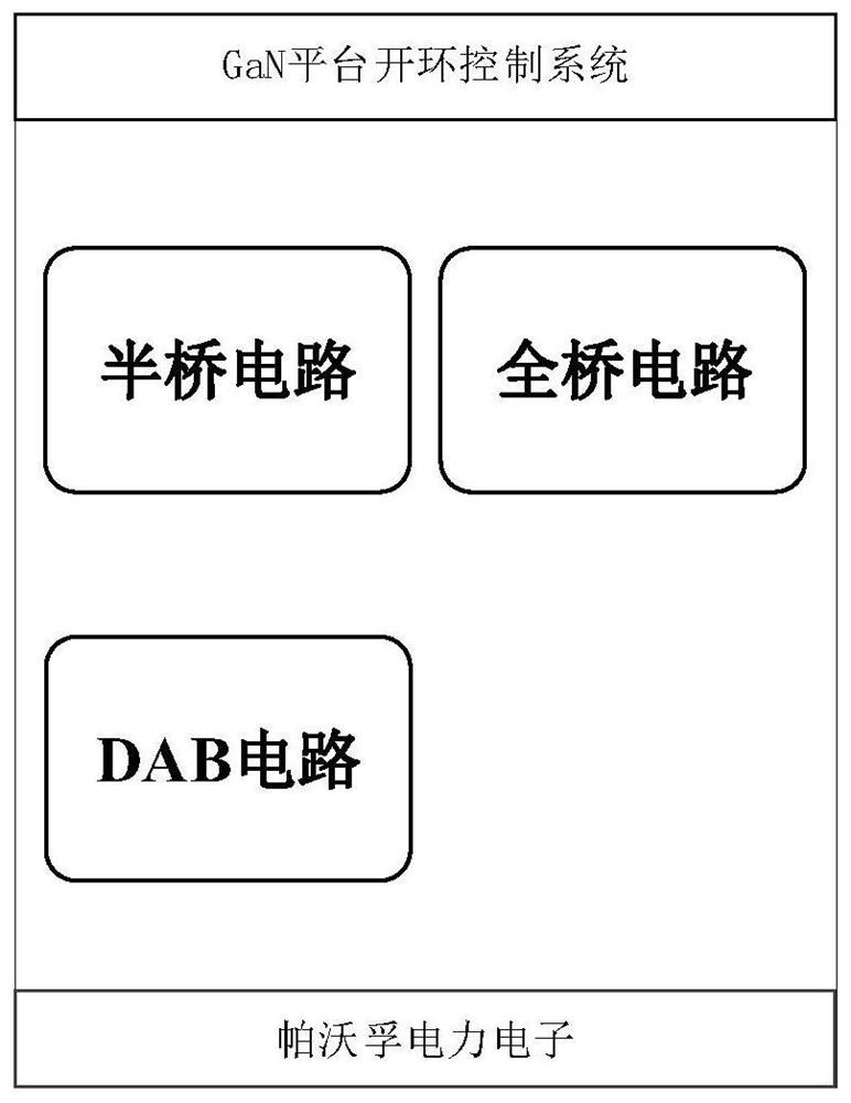
The invention discloses a universal experiment device of a power electronic circuit. The universal experiment device comprises an open loop controller, wherein a human-computer interaction module anda driving module are arranged in the open loop controller; the human-computer interaction module is connected with the driving module; the driving module is provided with four output connectors; eachoutput connector is connected with a BNC connector of a half-bridge mother board and a BNC connector of an H-bridge mother board; a half-bridge daughter board is inserted and connected onto the half-bridge mother board and the H-bridge mother board; and a proper number of capacitors and inductors are connected for respectively building half-bridge circuit topology, whole-bridge circuit topology and DAB circuit topology. The invention also discloses an experiment method of the experiment device. The experiment method is used for building the half-bridge circuit topology, the whole-bridge circuit topology and the DAB circuit topology. The device disclosed by the invention solves the problem of great device consumption, time waste and labor waste caused by the need of repeated circuit building in the existing circuit experiment; the utilization rate of the mother board is effectively improved; and the use of the whole device is convenient.

Description

technical field [0001] The invention belongs to the technical field of power electronics, and in particular relates to a general experimental device for power electronic circuits, and also relates to an experimental method for the experimental device. Background technique [0002] The application of power electronics technology is more and more extensive, and can be used in fields involving power conversion and transmission, such as power quality control, new energy power generation grid connection, special power supply, wireless charging, etc. Whether it is theoretical research or product development, it needs to be based on actual power electronic circuits. [0003] The construction process of power electronic circuits is relatively cumbersome, and the components in the circuit are difficult to reuse after the circuit is completed. For teaching in the field of power electronics, research and development of power electronics products, etc., where different circuits need to...

Claims


Application Information

Patent Timeline
Patent Type & Authority Patents(China)
IPC IPC(8): G09B23/18
CPCG09B23/188
Inventor 聂程徐玉石李鹏程
Owner 西安华谱电力设备制造有限公司
Learn More