Semiconductor device and method of forming the same

A semiconductor and device technology, applied in the field of semiconductor devices and their formation, can solve problems such as poor performance and achieve the effect of improving performance

Active Publication Date: 2021-02-02
SEMICON MFG INT (SHANGHAI) CORP +1
View PDF3 Cites 0 Cited by
  • Summary
  • Abstract
  • Description
  • Claims
  • Application Information

AI Technical Summary

Problems solved by technology

[0004] However, in the prior art, the performance of semiconductor devices composed of both planar MOS transistors and fin field effect transistors is poor.

Method used


Image

  • Semiconductor device and method of forming the same
  • Semiconductor device and method of forming the same
  • Semiconductor device and method of forming the same

Examples


Embodiment Construction

[0032] As mentioned in the background, semiconductor devices formed in the prior art have poor performance.

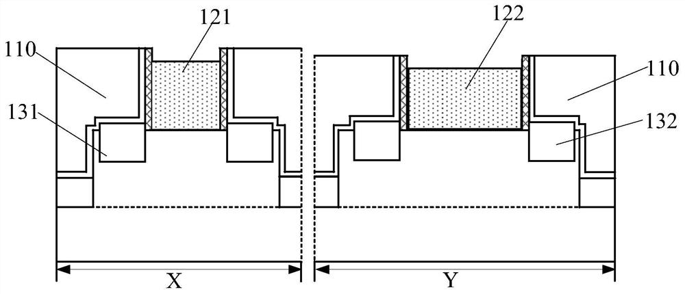
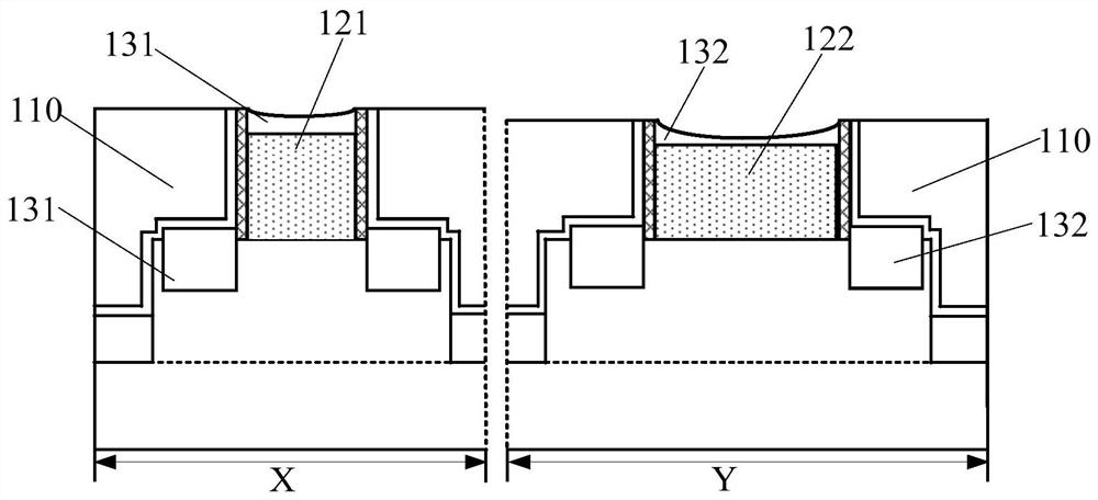
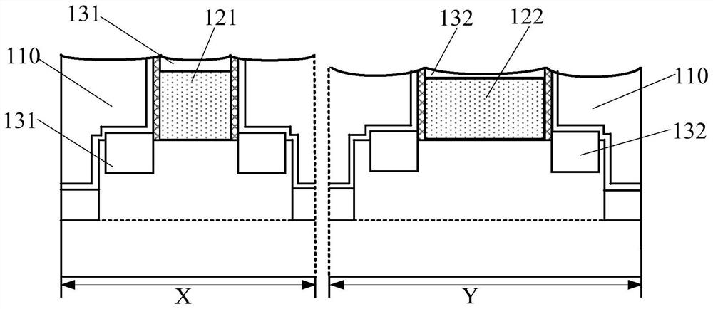
[0033] Figure 1 to Figure 3 It is a structural schematic diagram of the formation process of a semiconductor device.

[0034] refer to figure 1 , providing a substrate, the substrate includes a first region X and a second region Y, the first region X is used to form a short-channel transistor, the second region Y is used to form a long-channel transistor, the substrate has an underlying dielectric layer 110, the first The underlying dielectric layer 110 in the area X has a first groove penetrating through the underlying dielectric layer 110, and the second area Y has a second groove penetrating the underlying dielectric layer 110 in the underlying dielectric layer 110, and the width of the second groove is greater than that of the first groove. The width of the groove; the first gate structure 121 is formed in the first trench, and the top surface of the first gate ...


PUM

PropertyMeasurementUnit
sizeaaaaaaaaaa
sizeaaaaaaaaaa
depthaaaaaaaaaa

Abstract

A semiconductor device and its formation method include: formation of the first grid medium layer in the first groove and the first grid electrode located on the first grid medium layer;And the second grid electrode on the second grid medium layer; part of the first grid medium layer of the side wall of the first groove's side wall, forming the first depression between the first grid electrode and the first medium layer;Part of the second grid medium layer of the side wall of the two grooves forms a second depression between the second grid electrode and the first medium layer; the first protective layer and the second protection layer are formed.The second protection layer is located in the second depression; the first grid electrode and the second grid electrical stop layer are used to repair the surface of the first medium layer, as well as the top surface of the first protective layer and the top of the second protective layer.The method is improved the performance of semiconductor devices.

Description

technical field [0001] The invention relates to the field of semiconductor manufacturing, in particular to a semiconductor device and a forming method thereof. Background technique [0002] MOS transistors are one of the most important components in modern integrated circuits. The basic structure of a MOS transistor includes: a semiconductor substrate; a gate structure located on the surface of the semiconductor substrate, a source region located in the semiconductor substrate on one side of the gate structure, and a drain region located in the semiconductor substrate on the other side of the gate structure. The working principle of the MOS transistor is: by applying a voltage to the gate structure, the current through the channel at the bottom of the gate structure is adjusted to generate a switching signal. [0003] With the development of semiconductor technology, the ability of the traditional planar MOS transistor to control the channel current becomes weaker, resultin...

Claims


Application Information

Patent Timeline
Patent Type & Authority Patents(China)
IPC IPC(8): H01L21/8234H01L27/088
CPCH01L21/823431H01L21/823462H01L27/0886H01L21/823456H01L27/088H01L29/6653H01L29/66545H01L29/7848H01L21/02126H01L21/0214H01L21/0217H01L21/0228H01L21/28088H01L21/31055H01L21/76805H01L21/76895H01L21/823418H01L21/82345H01L21/823468H01L21/823475H01L23/535H01L29/42376H01L29/4966H01L29/4983H01L29/517H01L29/785
Inventor 王智东张城龙涂武涛
Owner SEMICON MFG INT (SHANGHAI) CORP
Why Eureka
Try Eureka