HEMT epitaxial structure and preparation method thereof

A technology of epitaxial structure and nano-nickel, which is applied in the field of HEMT epitaxial structure and its preparation, can solve the problems affecting the quality of HEMT, the quality of GaN layer crystal is not good enough, and the quality is not ideal, so as to improve the crystal quality, improve the quality, and have high material activity. Effect

Active Publication Date: 2019-07-09
HC SEMITEK ZHEJIANG CO LTD
View PDF4 Cites 2 Cited by
  • Summary
  • Abstract
  • Description
  • Claims
  • Application Information

AI Technical Summary

Problems solved by technology

However, due to the unsatisfactory quality of the AlN layer and the nano-nickel layer grown on the substrate, the crystal quality of the finally grown GaN layer is not good enough, which affects the quality of the HEMT.

Method used


Image

  • HEMT epitaxial structure and preparation method thereof
  • HEMT epitaxial structure and preparation method thereof
  • HEMT epitaxial structure and preparation method thereof

Examples


Embodiment Construction

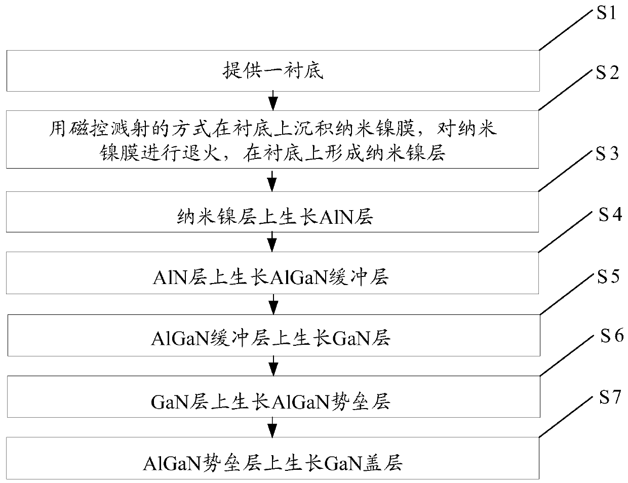
[0030] In order to make the object, technical solution and advantages of the present invention clearer, the implementation manner of the present invention will be further described in detail below in conjunction with the accompanying drawings.

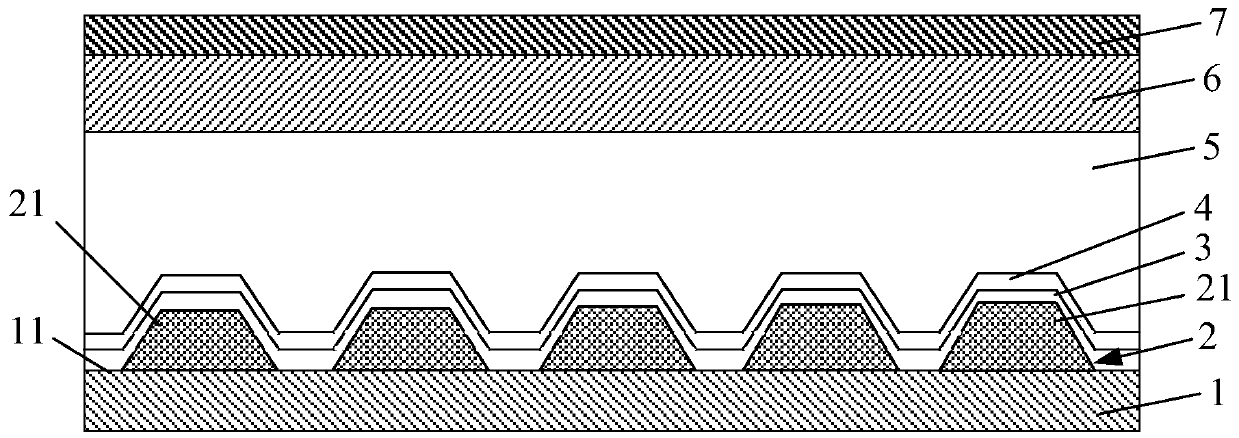
[0031] figure 1 It is a structural schematic diagram of a HEMT epitaxial structure provided by an embodiment of the present invention, such as figure 1 As shown, the HEMT epitaxial structure includes a substrate 1 and a nano-nickel layer 2 , an AlN layer 3 , an AlGaN buffer layer 4 , a GaN layer 5 , an AlGaN barrier layer 6 and a GaN capping layer 7 sequentially stacked on the substrate 1 .

[0032] The nano-nickel layer 2 includes a plurality of island-like structures 21 arranged on the substrate 1, and the plurality of island-like structures 21 are distributed on the substrate 1, and one surface of the layered nano-nickel layer 2 of the substrate 1 is the first surface 11. The projections of the island structures 21 on the first sur...


PUM

PropertyMeasurementUnit
thicknessaaaaaaaaaa
thicknessaaaaaaaaaa
thicknessaaaaaaaaaa

Abstract

The invention discloses an HEMT epitaxial structure and a preparation method thereof and belongs to the field of semiconductor photoelectric technologies. A nano-nickel layer has high material activity and can grow well on a substrate, and an AlN layer also can grow well on the nano-nickel layer; and the nano-nickel layer directly growing on the substrate can play a good role in connecting the substrate with the AlN layer, so that the quality of the AlN layer growing on the nano-nickel layer is improved beneficially. Since multiple island structures exist and each island structure has a certain slope, when the AlN layer gradually grows longitudinally, in the direction away from a first surface of the substrate, on the substrate, the AlN layer can grow laterally in the direction parallel tothe first surface at the same time. During longitudinal growth and lateral growth of the AlN layer, dislocation defects in different directions can be generated in the AlN layer; part of the dislocation defects generated during longitudinal growth of the AlN layer can offset part of the dislocation defects generated during lateral growth of the AlN layer; and through reduction of the defects, crystal quality of the AlN layer can be improved, and the quality of a finally obtained HEMT is improved.

Description

technical field [0001] The invention relates to the field of semiconductor optoelectronic technology, in particular to a HEMT epitaxial structure and a preparation method thereof. Background technique [0002] HEMT (High Electron Mobility Transistor, High Electron Mobility Transistor) is a heterojunction field effect transistor, which is widely used in various electrical appliances. The HEMT epitaxial structure is the basis for the preparation of HEMT devices. The current HEMT epitaxial structure includes a substrate and an AlN layer, a nano-nickel layer, a GaN layer, an AlGaN barrier layer, and a GaN capping layer stacked on the substrate in sequence. The substrate can be It is silicon carbide substrate, sapphire substrate or single crystal silicon substrate. [0003] Among them, the AlN layer and the nano-nickel layer can act as a buffer between the substrate and the GaN layer, improving the quality of the GaN layer grown on the silicon carbide substrate, sapphire substra...

Claims


Application Information

Patent Timeline
Patent Type & Authority Applications(China)
IPC IPC(8): H01L29/778H01L21/335
CPCH01L29/7786H01L29/66462
Inventor 丁涛周飚胡加辉李鹏
Owner HC SEMITEK ZHEJIANG CO LTD
Why Eureka
Try Eureka