Supercharge Your Innovation With Domain-Expert AI Agents!

Nano-imprinting device capable of preparing complex microstructure

A nano-imprint and micro-structure technology, which is applied in the direction of photomechanical equipment, pattern surface photolithography, optics, etc., to reduce costs, improve production efficiency, and reduce alignment and loading and unloading errors

Pending Publication Date: 2019-07-16
CHANGCHUN UNIV OF TECH
View PDF0 Cites 0 Cited by
  • Summary
  • Abstract
  • Description
  • Claims
  • Application Information

AI Technical Summary

Problems solved by technology

[0004] In order to solve the problem of preparing complex microstructures, the present invention proposes a nanoimprinting device capable of preparing complex microstructures

Method used


Image

  • Nano-imprinting device capable of preparing complex microstructure
  • Nano-imprinting device capable of preparing complex microstructure
  • Nano-imprinting device capable of preparing complex microstructure

Examples


Embodiment Construction

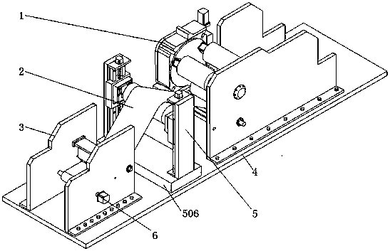
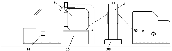
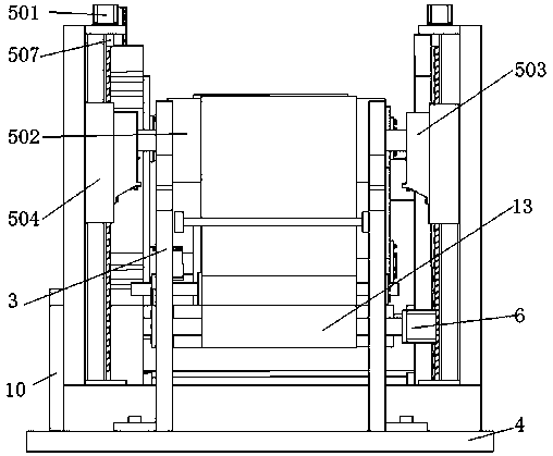
[0032] Such as figure 1 , figure 2 , image 3 , Figure 8As shown, the nanoimprinting device capable of preparing complex microstructures includes an imprinting device 1, a substrate 2, a frame 3, a bottom plate 4, an adjustment device 5, a servo motor 6, a winding roller 7, an engraved Erosion device 8, heating roller 9, loading block one 10, support roller 11, gluing device 12, unwinding roller 13, servo motor two 14. The frame 3 is connected to the bottom plate 4 by screws, the winding roller 7, the heating roller 9, the support roller 11, and the unwinding roller 13 are all fitted on the frame 3 through bearings, and the gluing box 1201 is fixed by screws On the frame 3, the servo motor 1 6 is connected with the unwinding roller 13, the servo motor 2 14 is connected with the winding roller 7, and the winding roller 7 and the unwinding roller 13 rotate synchronously, so that the substrate 2 advances smoothly, and the servo motor The first 6 and the servo motor two 14 a...


PUM


Abstract

The invention discloses a nano-imprinting device capable of preparing a complex microstructure. A method comprises the steps of firstly, unwinding a substrate by an unwinding roller; applying photoresist to the substrate by a glue application roller; conveying the substrate to the lower part of the imprinting device; heating the photoresist to a vitrification temperature by a heating roller; carrying out imprinting by an imprinting roller I, and then carrying out curing; removing a residual layer through an etching device; returning the substrate to the lower part of the imprinting device again, and then carrying out heating; rotating an imprinting roller II to the upper part of the photoresist subjected to the first-time imprinting by a rotating disc; carrying out imprinting by the imprinting roller II; and after imprinting by the imprinting roller II, repeating the steps until an imprinting roller III finishes imprinting, and winding the obtained substrate with the complex microstructure through a winding roller. According to the method, the complex microstructure is prepared through multi-roller imprinting, so that the complex micro-nanostructure can be rapidly and effectively prepared with relatively low cost; the method is simple; the device and processing realization cost is relatively low; a prepared pattern is relatively high in precision; an error is reduced; and the problems of damage on the pattern and a template on the substrate and high template replacement cost are avoided.

Description

technical field [0001] The invention relates to the field of nanoimprint photolithography, in particular to a nanoimprint device capable of preparing complex microstructures. Background technique [0002] With the continuous development of semiconductor technology, people have higher and higher specifications for electronic products. Under the guidance of Moore's Law, large-scale IC technology has entered the nanometer era. The widely used technology is lithography, including extreme ultraviolet lithography, electron beam direct writing, immersion lithography, etc. Due to the inherent defects of lithography technology and high cost, it is not suitable for mass production of large-scale electronic chips . In the next generation of image transfer technology, x-ray exposure, electron beam direct writing and nanoimprinting play an important role. Among them, nanoimprint technology was proposed by Professor Stephen Y.Chou of Princeton University at the end of the 20th century. ...

Claims


Application Information

Patent Timeline
Patent Type & Authority Applications(China)
IPC IPC(8): G03F7/00
CPCG03F7/0002
Inventor 谷岩卢明明林洁琼郑恭承张群李景鹏戴得恩易正发冯开拓王点正张哲名苍新宇徐梓苏付斌张晋
Owner CHANGCHUN UNIV OF TECH
Features
  • R&D
  • Intellectual Property
  • Life Sciences
  • Materials
  • Tech Scout
  • Unparalleled Data Quality
  • Higher Quality Content
  • 60% Fewer Hallucinations
Learn More