Touch/slip sensor and preparation method thereof, electronic equipment, braille identification equipment and robot
A sensor and tactile technology, applied in the field of sensing, can solve the problems of not having slippery perception, and achieve the effect of improving sensitivity and measuring range, and improving integration and stability
- Summary
- Abstract
- Description
- Claims
- Application Information
AI Technical Summary
Problems solved by technology
Method used
Image
Examples
Embodiment 1
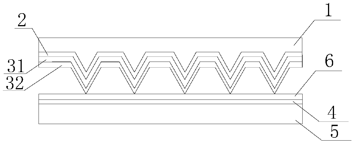
[0042] see figure 1 , is a schematic structural diagram of an embodiment of a capacitive touch / slip sensor of the present invention. Specifically, the capacitive touch / slip sensor of this embodiment includes from top to bottom:
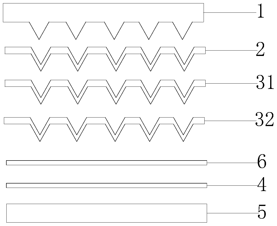
[0043] The first flexible substrate 1, the first electrode layer 2 with a micro-nano structure, the dielectric layer 3, the second electrode layer 4 and the second flexible substrate 5, wherein the first electrode layer 1 and the second electrode layer 3 are opposite set, and the dielectric layer 3 between the first electrode layer and the second electrode layer conformally integrates with the micro-nano structure of the first electrode layer 2 to form an electrode / dielectric layer integrated structure.
[0044] In this embodiment, the dielectric layer 3 is a composite dielectric layer formed by combining the flexible isolation layer 31 and the piezoelectric layer 32. Specifically, the flexible isolation layer 31 is made of flexible insulating materia...
Embodiment 2
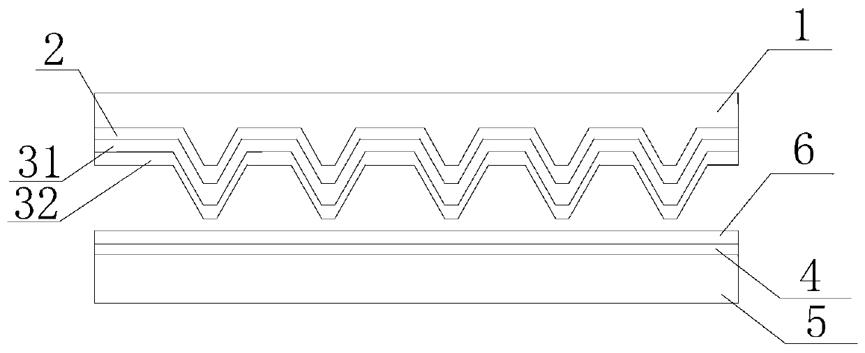
[0049] The present invention also provides another capacitive touch / slip sensor, which includes the various components in the first embodiment above, the difference is that the micro-nano structure on the first electrode layer in this embodiment is the first electrode The lower surface (that is, the surface in contact with the dielectric layer) periodically extends downwards, so that the first electrode layer 2 is approximately saw-toothed, see Figure 4 .
Embodiment 3
[0051] The present invention also provides another capacitive touch / slip sensor, which includes the various components in the first embodiment above, the difference is that in this embodiment, both the first electrode layer 2 and the second electrode layer 4 are A micro-nano structure is provided, and the protruding parts of the micro-nano structure on the first electrode layer 2 and the micro-nano structure on the second electrode layer are alternately arranged as Figure 5a As shown, or the raised part is set relative to, such as Figure 5b .
[0052] Of course, in this embodiment, both the first electrode layer and the second electrode layer can use graphene walls, and the preparation methods of the two are the same, that is, a wet etching process is used to etch a micron amount on the surface of the silicon substrate. level of multiple grooves; then use the PECVD method to generate graphene on the silicon substrate, and the growth time of graphene is controlled at 45-60 m...
PUM
| Property | Measurement | Unit |
|---|---|---|
| thickness | aaaaa | aaaaa |
| thickness | aaaaa | aaaaa |
| thickness | aaaaa | aaaaa |
Abstract
Description
Claims
Application Information


