Multilayer electronic part and method for producing the same

A technology of electronic components and multi-layer bodies, which is applied in transformer/inductor parts, inductance/transformer/magnet manufacturing, coil manufacturing, etc., can solve problems such as low pass rate, unstable size, and performance fluctuations, and achieve reduction Effects of performance fluctuation, elimination of terminal electrode distance fluctuation, and improvement of dimensional accuracy

Inactive Publication Date: 2003-01-29
TDK CORPARATION
View PDF6 Cites 4 Cited by
  • Summary
  • Abstract
  • Description
  • Claims
  • Application Information

AI Technical Summary

Problems solved by technology

like Figure 1D As shown, since the distance L1 between the terminal electrodes 7 has obvious fluctuations, not only the performance fluctuates obviously, but a

Method used


Image

  • Multilayer electronic part and method for producing the same
  • Multilayer electronic part and method for producing the same
  • Multilayer electronic part and method for producing the same

Examples


Embodiment Construction

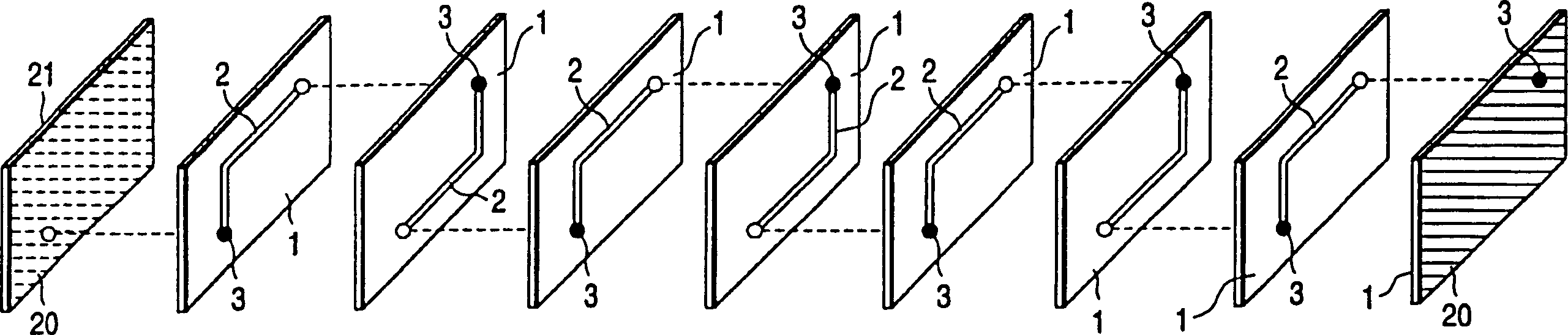
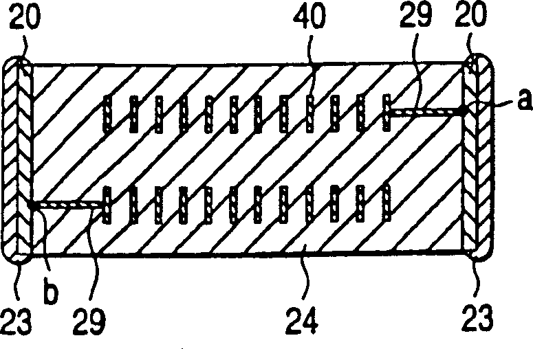
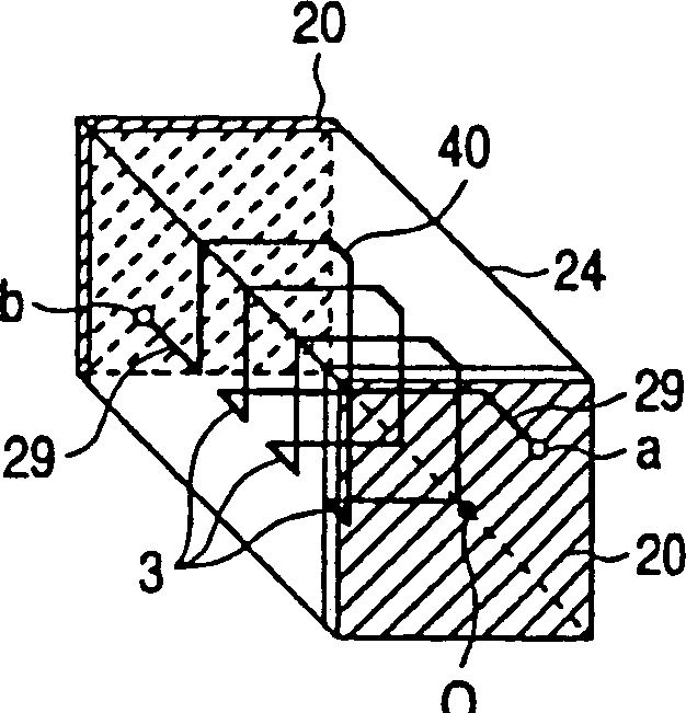
[0042] Figure 1A It is a perspective view corresponding to the layer structure of a chip as an embodiment of the electronic component of the present invention; Figure 1B with 1C are the cross-sectional and perspective views of the fabricated electronic components, respectively, Figure 1D is a plan view of electronic components mounted on a printed circuit board. figure 2 is a perspective view of the layer structure used to fabricate a plurality of chips of this embodiment. Figure 3A Perspective view of an assembly of stacked sheets. by Figure 1A Based on the layer structure shown, this embodiment of the electronic component was fabricated as follows.

[0043] A U (3 / 4 turn) or L (1 / 2 turn) shaped coil conductor 2 made of, for example, silver or silver alloy is printed on a green board 1 made of low magnetic permeability non-magnetic material. Form through hole 3 in each green board of these green boards 1 again, as Figure 1A As shown, the end of the coil conducto...


PUM


Abstract

A multilayer electronic part having the shape of a substantially rectangular parallelopiped is constituted which has a multilayer body formed by superposing coil conductors and green sheets of a magnetic or nonmagnetic material. Terminal electrodes are formed respectively on both ends of the multilayer body along the direction of the magnetic flux generating when current is caused to flow through the coil conductors in the multilayer body. The terminal electrodes each has a conductive substrate formed within the area of the end of the multilayer body and consisting of a lamination body as a component of the multilayer body.

Description

field of invention [0001] The present invention relates to a multilayer electronic component including an inductor formed by laminating a coil conductor and a magnetic or nonmagnetic material, and a method for manufacturing the same. And filters, resonators, etc. that are formed by inserting capacitors on top of inductors. Background technique [0002] Conventional multilayer electronic components are constructed as follows. Such as Figure 10A In the shown film layer structure, a coil conductor 2 is formed on a magnetic or non-magnetic material thin layer 1, and a through hole 3 is formed therein, and the thin layers with this structure are stacked. The components thus produced are fired and then diced into chips. As shown in FIG. 11A, these chips 4 are press-filled into through-holes 5a formed in a support plate 5 such as a silicon plate, after which both sides are dipped in silver paste 6. These chips 4 are plated with, for example, Ni or tin (Sn) after firing to form ...

Claims


Application Information

Patent Timeline
IPC IPC(8): H01F17/00H01F27/00H01F27/29H01F41/04H01G4/40H03H7/01H03H7/075
CPCH03H7/0115H01F17/0013H03H2001/0085Y10T29/49144Y10T29/49208Y10T29/43H03H2001/0057Y10T29/435H01F41/046H01F27/292Y10T29/49142Y10T29/49222Y10T29/49135Y10T29/49179Y10T29/49126H01F41/043Y10T29/4913Y10T29/49002Y10T29/49147H01F2017/0026
Inventor 熊谷修美阿部寿之小林诚齐藤则之柴田宪治佐佐木浩三高桥彻
Owner TDK CORPARATION
Why Eureka
Try Eureka