
An ultra-thin atomic force microscope probe

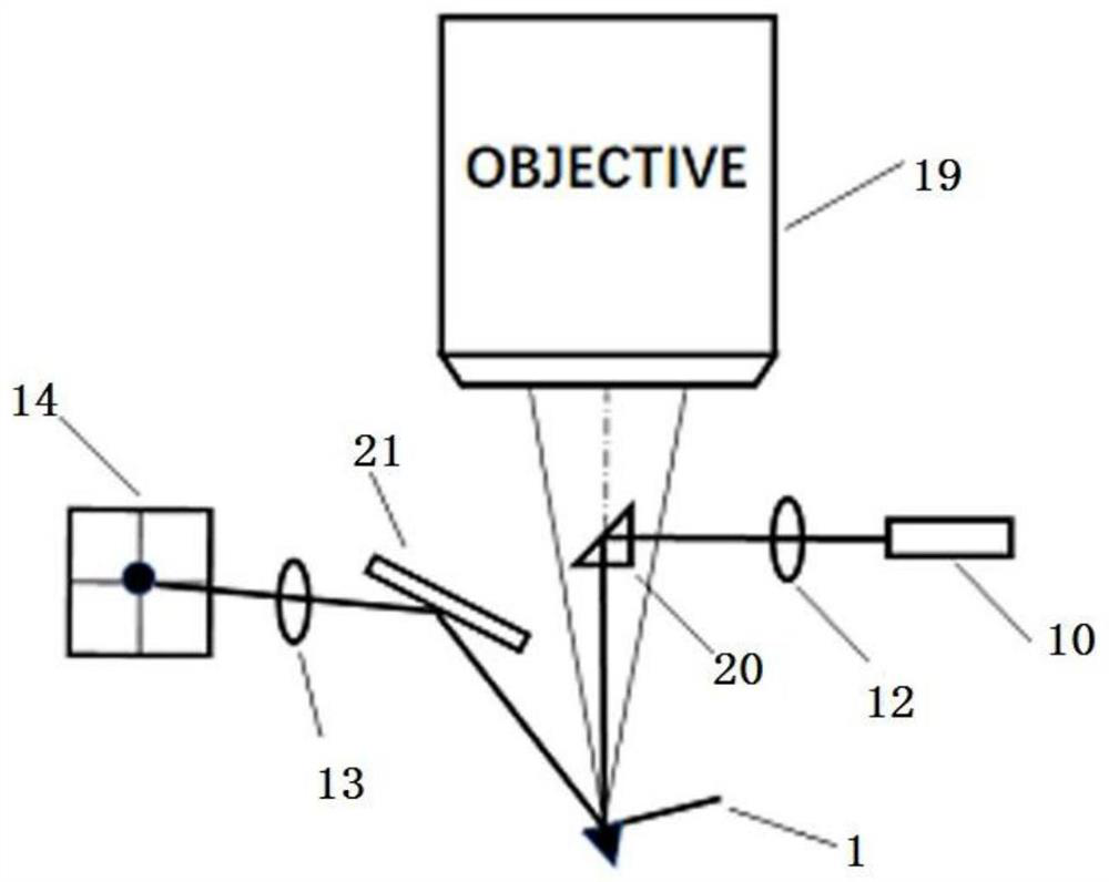
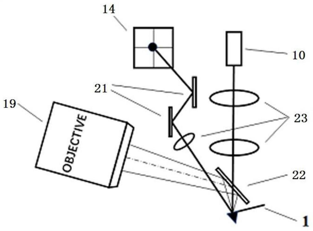
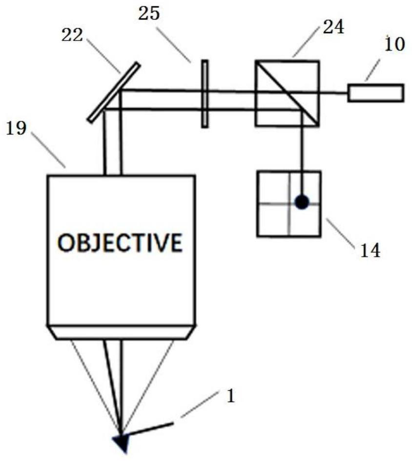
A measuring head and the same technology are applied in the direction of scanning probe microscopy, measuring devices, instruments, etc., and can solve the problems of large Z-direction space occupation and unfavorable integration of the atomic force microscope measuring head.

Active Publication Date: 2020-10-27
TIANJIN UNIV
View PDF7 Cites 0 Cited by
  • Summary
  • Abstract
  • Description
  • Claims
  • Application Information

AI Technical Summary

Problems solved by technology

[0006] As mentioned above, several existing optical path forms make the Z-direction space occupied by the probe part of the atomic force microscope too large, which is not conducive to the integration with optical microscopes (especially upright high-power optical microscopes), electron microscopes and other equipment

Method used


Image

  • An ultra-thin atomic force microscope probe
  • An ultra-thin atomic force microscope probe
  • An ultra-thin atomic force microscope probe

Examples


Embodiment 1

[0049] A probe fixing module, comprising: a cantilever beam probe 1, a piezoelectric ceramic 2, a probe holder 3, a first reflection surface 4, a first reflection device and a second reflection device, and the cantilever beam probe 1 is installed on In the probe holder 3, the tip of the cantilever beam probe 1 is located at the lowest point of the probe fixing module I, and the first reflective surface 4 is located on one side of the cantilever beam probe 1 for receiving the The laser 10 on one side emits a first laser beam and reflects the first laser beam to form a second laser beam, and the acute angle between the first reflecting surface 4 and the first laser beam is 60°-67.5°.

[0050] The first reflection device is located between the cantilever beam probe 1 and the first reflection surface 4, and the second laser beam is reflected by the first reflection device and irradiates on the cantilever beam probe 1 at an inclination angle of 45°-60° and is received by the cantile...

Embodiment 2

[0052] On the basis of Embodiment 1, an optical hole is formed between the first reflecting device and the second reflecting device for passing through the imaging optical path;

[0053] It also includes: a first adjustment frame 9 on which the first reflective surface 4 is installed, for adjusting the angle between the first reflective surface 4 and the first laser beam;

[0054] It also includes: a piezoelectric ceramic 2 fixed to the probe holder 3, used to excite the cantilever probe 1 to vibrate or scan in the Z direction (Z direction: the direction perpendicular to the first laser beam).

Embodiment 3

[0056] Such as Figure 5 As shown, on the basis of Embodiment 2, the first reflective device is a first reflective structure and a second reflective structure, the first reflective structure is a reflective surface, and the second reflective structure is a reflective surface. In this embodiment Among them, the first reflective structure is the second reflective surface 5, the second reflective structure is the third reflective surface 6, the first reflective structure and the second reflective structure are parallel to each other, the second reflective surface 5 and the third reflective surface 6 are respectively located at the The distance between the upper and lower sides of a laser beam is 3.7mm.

[0057] The second reflective device is a third reflective structure and a fourth reflective structure, the third reflective structure is a reflective surface, the fourth reflective structure is a reflective surface, the third reflective structure is a fourth reflective surface 7,...


PUM


Abstract

An ultra-thin atomic force microscope head. The atomic force microscope head employs an ultra-thin probe fixing module (I). The probe fixing module (I) comprises a cantilever probe (1), piezoelectric ceramic (2), a probe holder (3), a first reflecting surface (4), a first reflecting unit, and a second reflecting unit. The cantilever probe (1) is mounted in the probe holder (3), and the tip of the cantilever probe (1) is located at the lowest portion of the probe fixing module (I). The first reflecting surface (4) is located on one side of the cantilever probe (1). The first reflecting unit is located between the cantilever probe (1) and the first reflecting surface (4). The second reflecting unit is located between the cantilever probe (1) and a laser. A third laser beam is reflected by the second reflecting unit and then is emitted from the probe fixing module (I) to form a fourth laser beam. The Z-direction effective thickness of the probe fixing module (I) in the atomic force microscope head is only several millimeters, and therefore, the atomic force microscope head can be directly mounted below an optical or electron microscope having a working distance greater than the thickness to achieve integrated combination of different devices.

Description

technical field [0001] The invention belongs to the technical field of atomic force microscopes, and in particular relates to a probe fixing module with an ultra-thin vertical thickness and an atomic force microscope measuring head based on the probe fixing module. Background technique [0002] The emergence of atomic force microscopes in the 1980s enabled people to break through the limitations of traditional optical microscopes imposed by the diffraction limit, and to achieve three-dimensional characterization of various materials with sub-nanometer resolution. Not only that, this technology can also perform in-situ detection of physical properties of materials and even manipulation and processing at the atomic level. After more than 30 years of development, the atomic force microscope has been widely used in the semiconductor industry, new materials, life sciences and other fields, and is one of the necessary tools for scientific research at the micro-nano scale. [0003...

Claims


Application Information

Patent Timeline
Patent Type & Authority Patents(China)
IPC IPC(8): G01Q60/24G01Q60/38
CPCG01Q60/24G01Q60/38
Inventor 吴森卢念航胡晓东
Owner TIANJIN UNIV
Learn More