
Graphene-based tunneling field effect transistor unit, array and method for forming the same

A technology of tunneling field effect and graphene, which is applied in the direction of electrical components, circuits, semiconductor devices, etc., can solve the problems that are difficult to realize large-scale integration applications, and achieve large-scale device integration applications, precise unit site selection, high switching than the effect

Active Publication Date: 2016-01-20
SHANGHAI INST OF MICROSYSTEM & INFORMATION TECH CHINESE ACAD OF SCI
View PDF6 Cites 0 Cited by
  • Summary
  • Abstract
  • Description
  • Claims
  • Application Information

AI Technical Summary

Problems solved by technology

[0005] In view of the above-mentioned shortcoming of the prior art, the object of the present invention is to provide a graphene-based tunneling field effect transistor unit, array and forming method thereof, for solving the switching ratio of the graphene field effect transistor in the prior art Low-level problems that are difficult to achieve large-scale integrated applications

Method used


Image

  • Graphene-based tunneling field effect transistor unit, array and method for forming the same
  • Graphene-based tunneling field effect transistor unit, array and method for forming the same
  • Graphene-based tunneling field effect transistor unit, array and method for forming the same

Examples


Embodiment 1

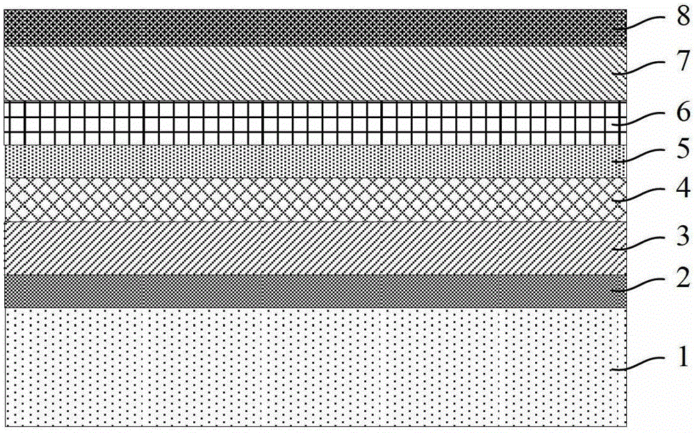
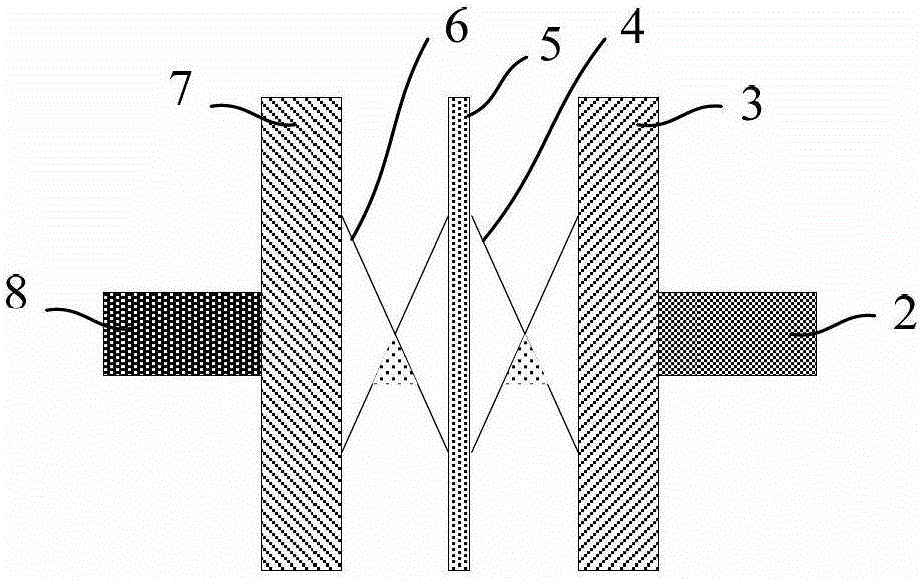
[0058] The present invention provides a graphene-based tunneling field effect transistor unit, please refer to figure 1 , shown as a schematic diagram of the graphene-based tunneling field effect transistor unit, as shown in the figure, the unit at least includes a substrate 1; the substrate 1 includes a bottom gate electrode 2, a first Dielectric layer 3, bottom graphene 4, insulating barrier layer 5, top graphene 6, second dielectric layer 7 and top gate electrode 8; the bottom graphene 4 and the top graphene 6 are ribbon graphene or graphite Graphene nanobelts; the width of the ribbon-shaped graphene is greater than 100nm; the width of the graphene nanobelts is in the range of 1 to 100nm.

[0059] Specifically, the substrate 1 is a conventional insulating substrate such as SiO 2 , MgO, diamond-like carbon film (DLC), etc., can also be other flexible substrates such as PET, etc. The insulating barrier layer 5 is a few-layer hexagonal boron nitride film or a molybdenum disu...

Embodiment 2

[0067] see Figure 4 and Figure 5 , the present invention provides a graphene-based tunneling field effect transistor array, wherein, Figure 4 Shown as a perspective schematic diagram of a graphene-based tunneling field effect transistor array of the present invention, Figure 5 Shown is a top view of the graphene-based tunneling field effect transistor array of the present invention.

[0068] Such as Figure 4 As shown, the graphene-based tunneling field effect transistor array includes a substrate 1; the substrate 1 is a conventional insulating substrate such as SiO 2 , MgO, diamond-like carbon film (DLC), etc., can also be other flexible substrates such as PET, etc.

[0069] The graphene-based tunneling field effect transistor array also includes at least two bottom gate electrodes 2 arranged in parallel in the longitudinal direction, and the bottom gate electrodes 2 are formed on the substrate 1; wherein, the parallel arrangement in the longitudinal direction refers ...

Embodiment 3

[0085] see Figure 6 ~ Figure 11 and Figure 5 , the present invention also provides a method for forming a graphene-based tunneling field effect transistor array, characterized in that the method at least includes the following steps:

[0086] Step 1), see Image 6 , providing a substrate 1 on which at least two bottom gate electrodes 6 arranged in parallel longitudinally are formed.

[0087] Specifically, the substrate 1 is a conventional insulating substrate such as SiO 2 , MgO, diamond-like carbon film (DLC), etc., can also be other flexible substrates such as PET, etc. The material of the bottom gate electrode 6 is conductive metal such as Au, Ag, Pt, Cu, Al. In order to facilitate contact, the width of the contact part at both ends of the bottom gate electrode can be greater than the width of the middle part, which can be dumbbell-shaped. For the convenience of illustration, the width of the contact part at both ends of the bottom gate electrode in the figure is cons...


PUM

PropertyMeasurementUnit
widthaaaaaaaaaa
thicknessaaaaaaaaaa
thicknessaaaaaaaaaa

Abstract

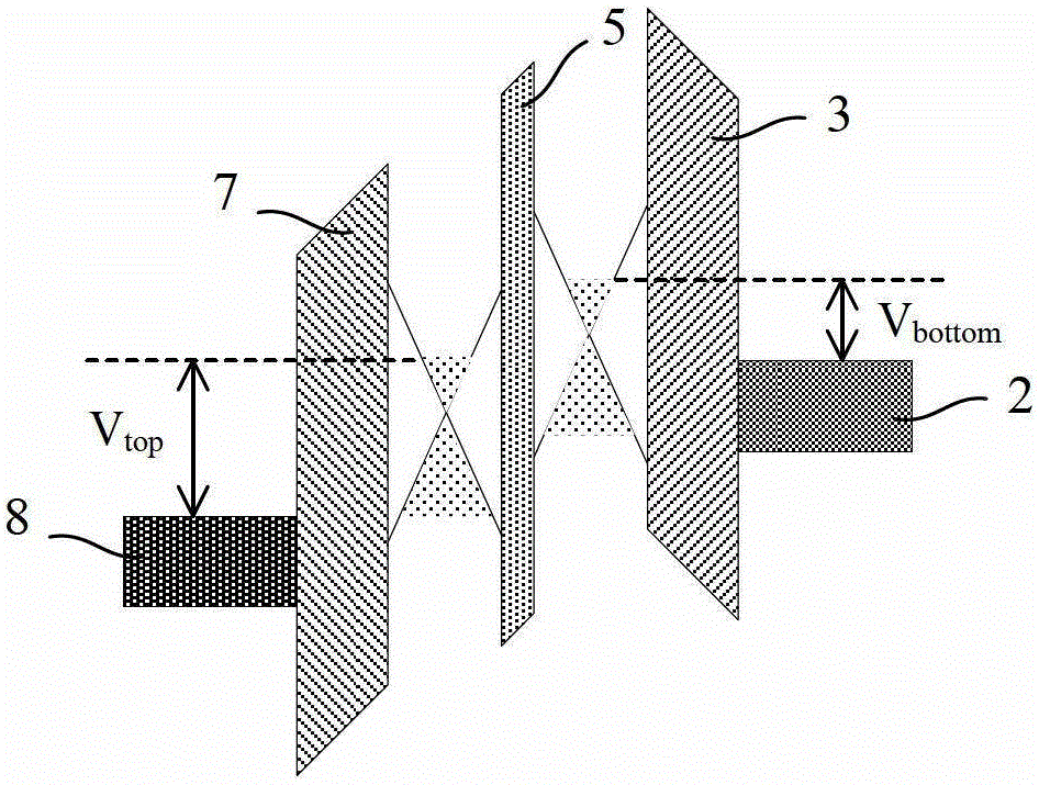
The invention provides a graphene-based tunneling field-effect transistor unit and array and a forming method of the array. The unit at least comprises a substrate, wherein the substrate sequentially comprises a bottom grid electrode, a first dielectric layer, a bottom graphene layer, an insulating barrier layer, a top graphene layer, a second dielectric layer and a top grid electrode which are arranged from the bottom up; the bottom graphene layer and the top graphene layer are both banded graphene or graphene nanoribbon; the width of the banded graphene is larger than 100 nm; the width of the graphene nonaribbon ranges from 1 nm to 100 nm. As the insulating barrier layer is led between the bottom graphene layer and the top graphene layer, the concentrations of carriers in the bottom graphene layer and the top graphene layer can be respectively adjusted through voltages added on the bottom grid electrode and the top grid electrode, and accordingly, higher on-off ratio is realized; meanwhile, as the top grid electrode and the bottom grid electrode can achieve accurate unit site selection, large-scale device integrated application is realized.

Description

technical field [0001] The invention belongs to the technical field of semiconductors and relates to a field effect transistor, in particular to a graphene-based tunneling field effect transistor unit, an array and a forming method thereof. Background technique [0002] Since the discovery of single-layer graphite by the Novoselov and Geim groups at the University of Manchester in 2004 [K.S. Novoselov, A.K. Geim, S.V. Morozov, D. Jiang, Y. Zhang, S.V. Dubonos, I.V. 666(2004)], the research on graphene has aroused people's widespread attention. Graphene has unique physical properties that other members of the carbon family do not possess, such as the anomalous integer quantum Hall effect, the finite conductance of intrinsic graphene, and universal photoconductivity. Taking advantage of these interesting physical properties, graphene can be used in the design of novel transistor devices. [0003] Since the single-layer graphite with a planar structure can be easily manipulat...

Claims


Application Information

Patent Timeline
Patent Type & Authority Patents(China)
IPC IPC(8): H01L29/78H01L29/49H01L21/336H01L21/28
Inventor 王浩敏谢红吴天如孙秋娟王慧山宋阳曦刘晓宇唐述杰谢晓明
Owner SHANGHAI INST OF MICROSYSTEM & INFORMATION TECH CHINESE ACAD OF SCI
Learn More