Display panel

A technology for display panels and touch wiring, applied in optics, instruments, electrical components, etc., can solve problems such as abnormal data transmission of display panels, and achieve the effect of avoiding short-circuit and improving yield

Active Publication Date: 2019-07-23
WUHAN CHINA STAR OPTOELECTRONICS TECH CO LTD
View PDF6 Cites 8 Cited by
  • Summary
  • Abstract
  • Description
  • Claims
  • Application Information

AI Technical Summary

Problems solved by technology

[0005] The invention provides a display panel to solve the technical problem of abnormal data transmission of the existing display panel

Method used


Image

  • Display panel
  • Display panel
  • Display panel

Examples


Embodiment Construction

[0047] The following descriptions of the various embodiments refer to the accompanying drawings to illustrate specific embodiments in which the invention may be practiced. The directional terms mentioned in the present invention, such as [top], [bottom], [front], [back], [left], [right], [inside], [outside], [side], etc., are only for reference The orientation of the attached schema. Therefore, the directional terms used are used to illustrate and understand the present invention, but not to limit the present invention. In the figures, structurally similar elements are denoted by the same reference numerals.

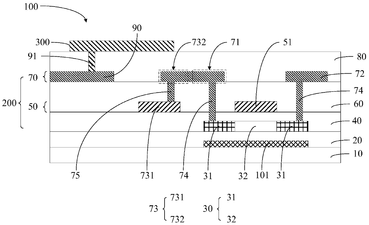
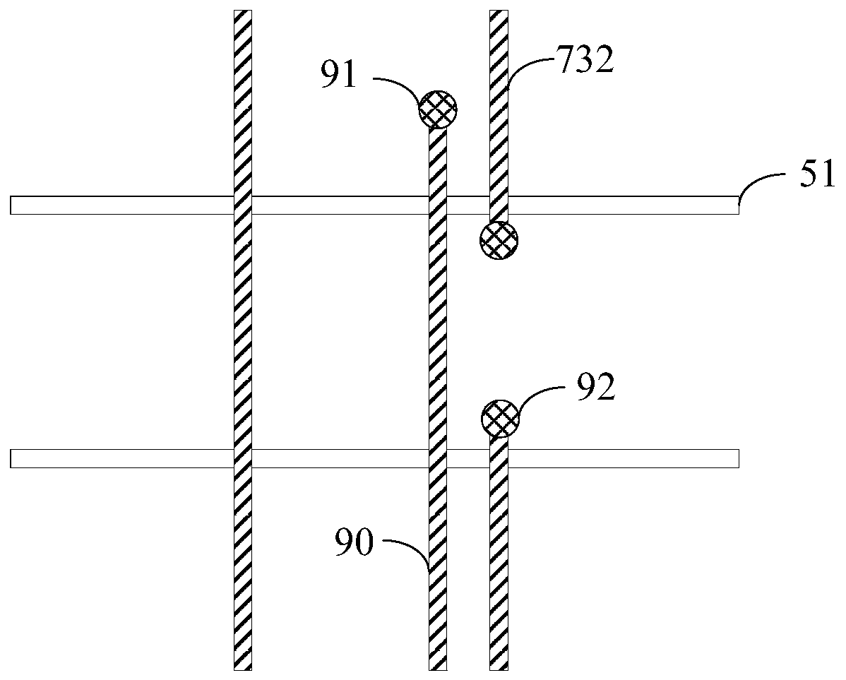
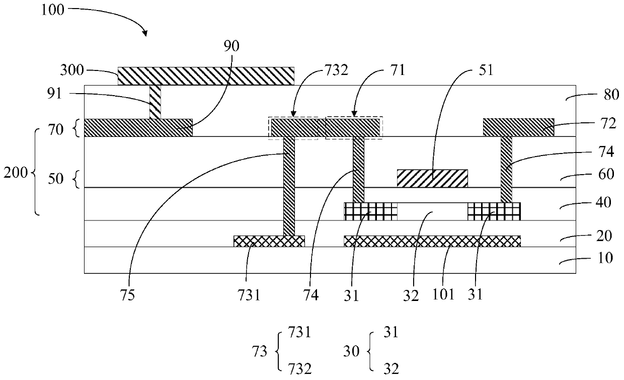
[0048] see figure 1 , figure 1 It is the first structure diagram of the display panel 100 of the present application.

[0049] The display panel 100 includes a substrate 10 , a TFT layer 200 on the substrate 10 , and a touch layer 300 on the TFT layer 200 .

[0050] In this embodiment, the raw material of the substrate 10 may be one of a glass substrate, a quartz su...


PUM


Abstract

The invention proposes a display panel. The display panel comprises a substrate, a thin film transistor layer and a touch control layer, wherein the thin film transistor layer is arranged on the substrate, the touch control layer is arranged on the thin film transistor layer, the thin film transistor layer comprises a source-drain layer, a source / drain and a data signal line are arranged on the source-drain layer, the display panel also comprises a touch control wire, the touch control wire is electrically connected with the touch control layer and is arranged between the substrate and the touch control layer, and a part of data signal line and a part of touch control wire are not arranged at the same layer. A part, at relatively small distance with the data signal line, of the touch control wire is arranged on different film layers by a jumper design, short connection of the touch control wire and the data signal line is prevented, a data signal is normally transmitted, and the product yield is improved.

Description

technical field [0001] The invention relates to the display field, in particular to a display panel. Background technique [0002] Low temperature polysilicon (LTPS), due to its high electron mobility, can effectively reduce the area of ​​thin film transistor (Thin Film Transistor, TFT) devices, thereby increasing the aperture ratio of pixels and increasing the panel display Brightness can reduce the overall power consumption at the same time, so that the manufacturing cost of the panel is greatly reduced, and it has become a hot technology in the field of liquid crystal display. [0003] In the display panel in the prior art, in order to save the photomask, the touch leads and the source and drain layers are often arranged on the same layer. Due to the shortage of wiring space, the touch leads and the data lines are short-circuited, which affects the data transmission performance of the display panel, resulting in The abnormal display of the display panel reduces the yield...

Claims


Application Information

Patent Timeline
Patent Type & Authority Applications(China)
IPC IPC(8): H01L27/12G02F1/1333G02F1/1362
CPCG02F1/13338G02F1/136286G02F1/13629H01L27/1214H01L27/124
Inventor 卢改平崔珠峰
Owner WUHAN CHINA STAR OPTOELECTRONICS TECH CO LTD
Why Eureka
Try Eureka