Semiconductor gas sensor and preparation method thereof
A gas sensor and semiconductor technology, which is applied in the field of micro-thin film gas sensor preparation, can solve the problems of poor gas sensitivity and achieve the effect of improving sensitivity and simple method
- Summary
- Abstract
- Description
- Claims
- Application Information
AI Technical Summary
Problems solved by technology
Method used
Image
Examples
Embodiment 1
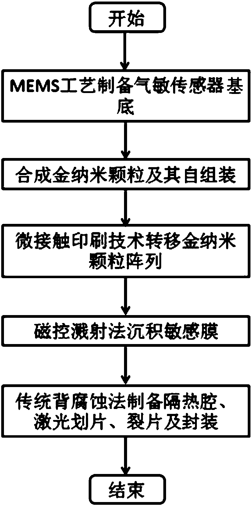
[0081] The preparation process of the semiconductor gas sensor provided in this embodiment is as follows: figure 2 Shown, preparation method comprises the steps:
[0082] (1) The sensor substrate is made by MEMS technology, including Si 3 N 4 / Si substrate cleaning, photolithography to make Pt heating resistors, deposition of silicon oxide insulating layer, optical exposure to make interdigital electrodes, and exposure of gold interdigital electrode areas through conventional photolithography processes.
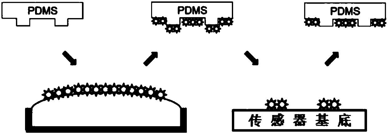
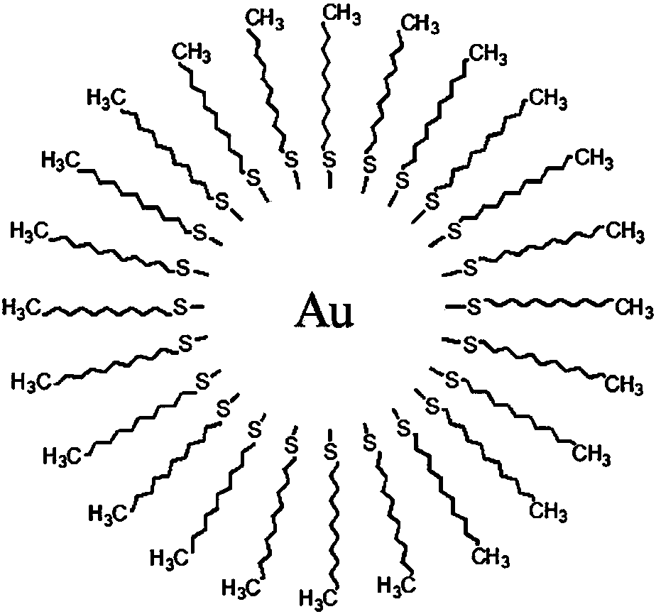
[0083] (2) Prepare 10nm gold nanoparticles and coat them with dodecyl mercaptan molecules, self-assemble at the water / air interface, and transfer them to the sensor substrate with a PDMS stamp; use 100W power magnetron sputtering of SnO 2 / NiO target for 430s to obtain SnO with a thickness of about 20nm 2 / NiO film, where, image 3 A schematic diagram of the structure of gold nanoparticles coated with dodecyl mercaptan molecules is given, Figure 4 A schematic diagram o...
Embodiment 2
[0088] The preparation method of the semiconductor gas sensor provided in this embodiment comprises the following steps:
[0089] (1) The sensor substrate is made by MEMS technology, including Si 3 N 4 / Si substrate cleaning, photolithography to make Pt heating resistors, deposition of silicon oxide insulating layer, optical exposure to make gold finger electrodes, and expose the gold finger electrode area through conventional photolithography process.
[0090] (2) Prepare 10nm gold nanoparticles and coat them with dodecyl mercaptan molecules, self-assemble the gold nanoparticles in the LB tank, insert the sensor substrate into the LB tank and pull it slowly, large-area long-range ordered gold nanoparticles Particle arrays were transferred onto the sensor substrate; SnO was magnetron sputtered using a power of 100W 2 Target 860s, get SnO with a thickness of about 40nm 2 film.
[0091] (3) Soak the sensor substrate in acetone for 5 minutes to remove the residual photoresist...
Embodiment 3
[0095] The only difference from Example 1 is that the gas-sensitive thin film deposited in this example is 20nm WO 3 Except for the film, other preparation methods and conditions are the same as in Example 1.
[0096] The yield rate of the acetone sensor obtained in this embodiment is >95%, and the consistency deviation is <10%.
PUM
| Property | Measurement | Unit |
|---|---|---|
| diameter | aaaaa | aaaaa |
| thickness | aaaaa | aaaaa |
| thickness | aaaaa | aaaaa |
Abstract
Description
Claims
Application Information
 - R&D
- Intellectual Property
- Life Sciences
- Materials
- Tech Scout
- Unparalleled Data Quality
- Higher Quality Content
- 60% Fewer Hallucinations
Browse by: Latest US Patents, China's latest patents, Technical Efficacy Thesaurus, Application Domain, Technology Topic, Popular Technical Reports.
© 2025 PatSnap. All rights reserved.Legal|Privacy policy|Modern Slavery Act Transparency Statement|Sitemap|About US| Contact US: help@patsnap.com


