Flexible touch panel

A flexible touch and panel technology, applied in instruments, electrical digital data processing, input/output process of data processing, etc., can solve the problems of difficult oncell implementation, complex structure, and high process difficulty, avoiding signal interference and excessive concentrated effect

Active Publication Date: 2019-07-26
WUHAN CHINA STAR OPTOELECTRONICS SEMICON DISPLAY TECH CO LTD
View PDF6 Cites 5 Cited by
  • Summary
  • Abstract
  • Description
  • Claims
  • Application Information

AI Technical Summary

Problems solved by technology

Among them, the mutual capacitance type needs to use two layers of driving and sensing electrodes. For example, the mutual capacitance structure in an oncell needs to complete the bridging design where the driving electrode and the sensing electrode overlap. The process is difficult and the structure is complex.
Among them, the self-capacitance type only needs a single layer of electrodes, no bridging is required, the process is less, and the structure is simple. The touch di

Method used


Image

  • Flexible touch panel
  • Flexible touch panel
  • Flexible touch panel

Examples


Example Embodiment

[0047] Example

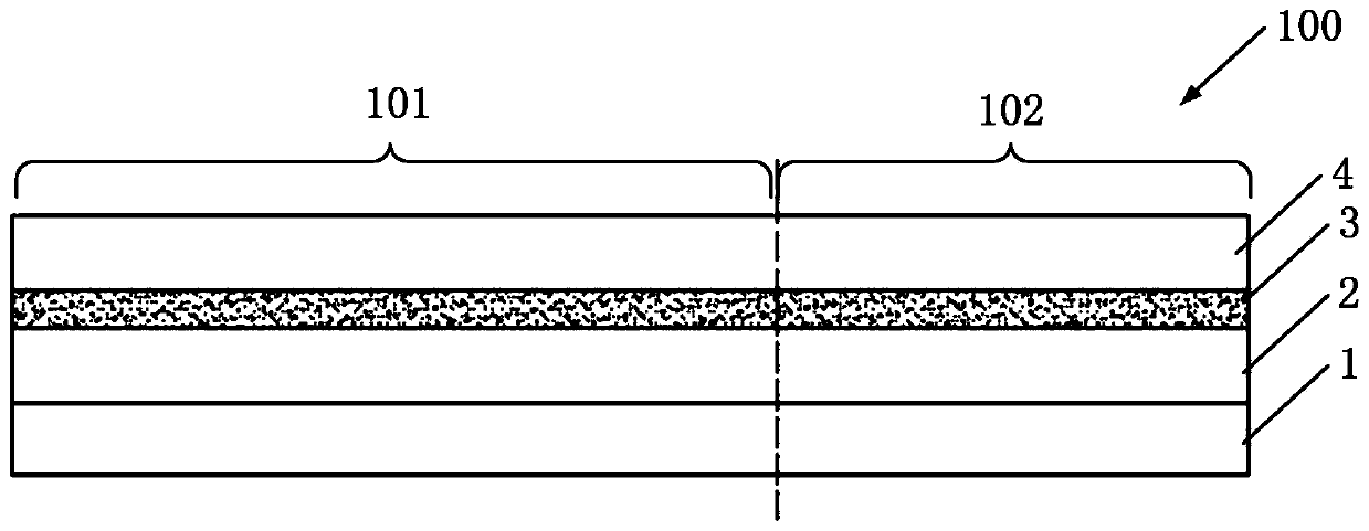
[0048] Such as figure 1 As shown, a flexible touch panel 100 is defined with a first area 101 and a second area 102, where the first area 101 is a display area. The flexible touch panel 100 includes a substrate 1, an OLED encapsulation layer 2, a touch electrode metal layer 3 and a touch encapsulation layer 4. The OLED encapsulation layer 2 is disposed on the substrate 1; the touch electrode metal layer 3 is disposed on the OLED encapsulation layer 2; the touch encapsulation layer 4 is disposed on the touch electrode metal layer 3 on.

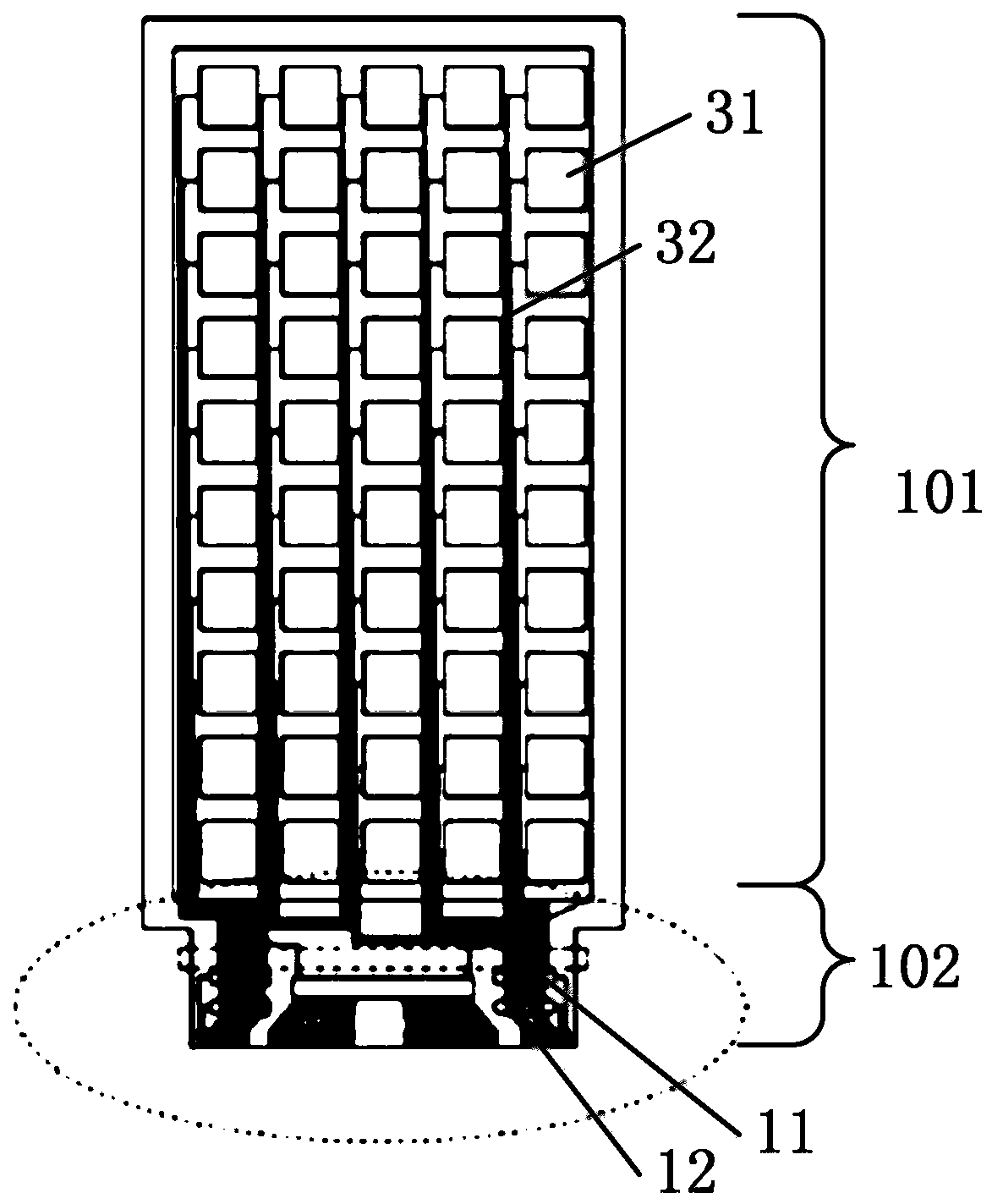
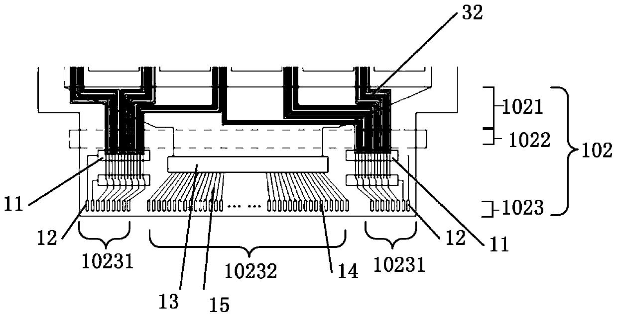
[0049] Such as figure 2 As shown, the touch electrode metal layer 3 at the position of the first area 101 is provided with a touch unit 31, and a high-speed switch controller is provided on the substrate 1 at the position of the second area 102 11 and the touch bonding terminal 12; wherein the touch unit 31 is connected to the touch bonding terminal 12 through the high-speed switch controller 11 through a touch sensing signal lea...


PUM


Abstract

The invention relates to a flexible touch panel. The flexible touch panel comprises a substrate, an OLED packaging layer, a touch electrode metal layer and a touch packaging layer. According to the invention, self-capacitance touch electrodes are manufactured on the flexible touch panel. A high-speed switch controller is additionally arranged in the second area. Touch sensing signal leads are processed by the high-speed switch controller, and under the condition that the number of the touch units is not changed, the number of the touch sensing signal leads led out to touch bonding terminals isreduced, so that the position of a display bonding area is reserved, and the touch sensing signal leads can be conveniently realized on an oncell. Therefore, the display bonding area is separated from the touch bonding area, excessive concentration of the touch sensing signal leads and the display signal leads is avoided, and signal interference is avoided.

Description

technical field [0001] The invention relates to the field of display technology, in particular to a flexible touch panel. Background technique [0002] The display device can convert the data of the computer into various characters, numbers, symbols or intuitive images and display them, and can use keyboard and other input tools to input commands or data into the computer, and add, delete, modify and change the display at any time with the help of the system's hardware and software. content. Display devices are classified into plasma, liquid crystal, light emitting diode, and cathode ray tube according to the display device used. [0003] OLED (full name in English: Organic Light-Emitting Diode, Organic Light-Emitting Diode) display device is also called organic electro-laser display device, organic light-emitting semiconductor. The basic structure of an OLED is a thin, transparent indium tin oxide (ITO) with semiconducting properties connected to the positive electrode of...

Claims


Application Information

Patent Timeline
IPC IPC(8): G06F3/041G06F3/044
CPCG06F3/0412G06F3/0416G06F3/044G06F2203/04102G06F2203/04112
Inventor 陈碧
Owner WUHAN CHINA STAR OPTOELECTRONICS SEMICON DISPLAY TECH CO LTD
Why Eureka
Try Eureka