TFT array substrate and display panel

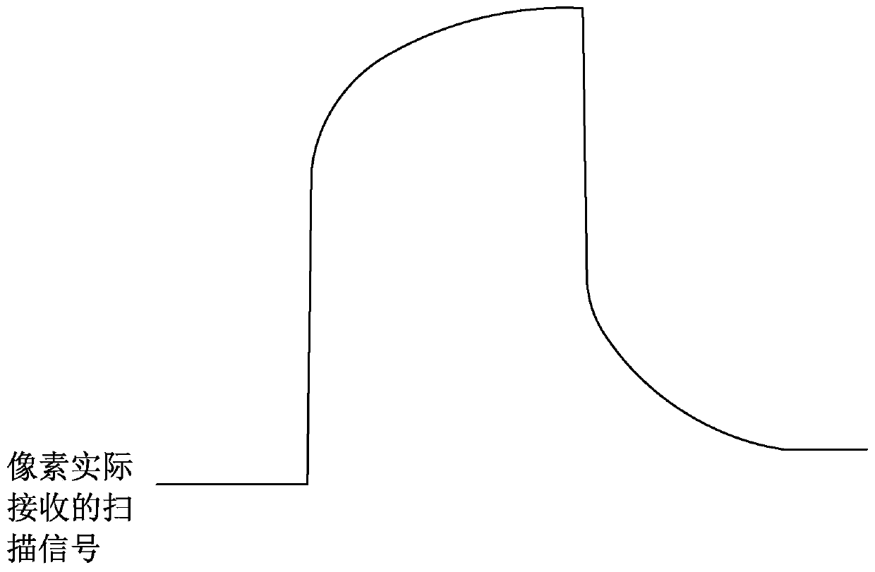
A technology for array substrates and display areas, applied in static indicators, optics, instruments, etc., can solve problems such as prolonged rise time and fall time of scanning signals, influence on screen display, wrong pixel charging, etc., to shorten fall time and ensure display quality effect

Active Publication Date: 2019-07-30
SHENZHEN CHINA STAR OPTOELECTRONICS SEMICON DISPLAY TECH CO LTD
View PDF5 Cites 5 Cited by
  • Summary
  • Abstract
  • Description
  • Claims
  • Application Information

AI Technical Summary

Problems solved by technology

In the prior art, the scan signal is pulled down by the pull-down unit inside the GOA circuit 500. However, when the GOA circuit 500 transmits the scan signal to the pixel 200 of the effective display area 110 through the scan line 300, a large amount of capacitance and resistance will inevitably be generated. , under the action of these capacitors and resistors, the rising time and falling time of the scanning signal will be lengthened, and the situation of the falling time being prolonged is extremely serious, so please refer to figure 2 , the waveform of the scanning signal actually received by the pixel 200 will be severely distorted, and driving errors will occur, resulting in wrong charging of the pixels and affecting the display of the screen

Method used


Image

  • TFT array substrate and display panel
  • TFT array substrate and display panel
  • TFT array substrate and display panel

Examples


Embodiment Construction

[0037] In order to further illustrate the technical means adopted by the present invention and its effects, the following describes in detail in conjunction with preferred embodiments of the present invention and accompanying drawings.

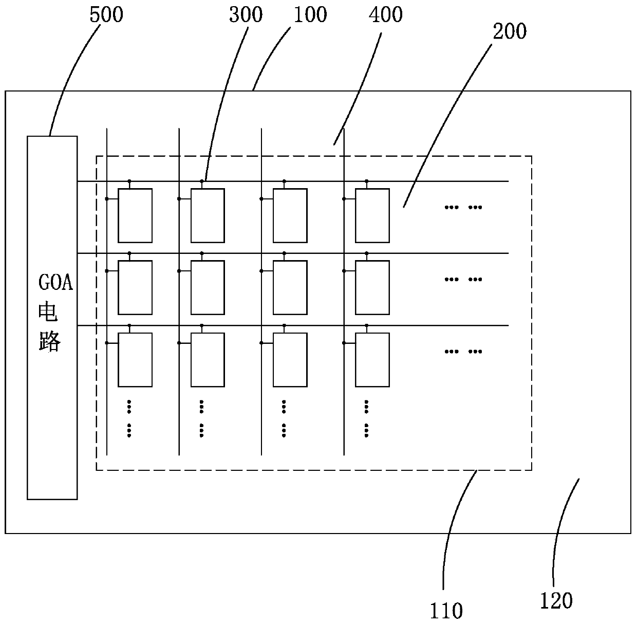
[0038] see image 3 , the present invention provides a TFT array substrate, including a substrate 10, a plurality of pixels 20 disposed on the substrate 10, and a plurality of scanning lines 30 (GATE (1), GATE (2) sequentially disposed on the substrate 10 , . . . , GATE(N), GATE(N+1), GATE(N+2), . . . , GATE(last)) and the GOA circuit 40 disposed on the substrate 10.

[0039] The plurality of pixels 20 are arranged in an array. The GOA circuit 40 is located outside the area where the pixels 20 are located. A plurality of scan lines 30 are connected to the GOA circuit 40 , and each scan line 30 is electrically connected to a row of pixels 20 . Each pixel 20 includes a first thin film transistor T1. Except for the last row of pixels 20, the g...


PUM


Abstract

The invention provides a TFT array substrate and a display panel. According to the TFT array substrate provided by the present invention, a first thin film transistor is disposed in each pixel, and the grid electrode of the first thin film transistor in the Nth row of pixels is electrically connected with the (N+1)th scanning line. The drain electrode is electrically connected with the Nth scanning line, the source electrode is connected with the negative voltage of the power supply, and therefore a scanning signal received by each pixel is independently pulled down in each pixel, thereby greatly shortening the falling time of the scanning signal and being beneficial to ensuring the display quality of the display panel.

Description

technical field [0001] The invention relates to the field of display technology, in particular to a TFT array substrate and a display panel. Background technique [0002] Flat panel display devices such as Liquid Crystal Display (LCD) and Organic Light Emitting Display (OLED) have many advantages such as thin body, power saving, and no radiation, and have been widely used. Such as: LCD TV, mobile phone, personal digital assistant (PDA), digital camera, computer screen or laptop screen, etc. [0003] GOA (Gate Driver on Array) technology is the array substrate row drive technology, which uses the thin film transistor (Thin Film Transistor, TFT) array process to manufacture the gate scanning drive circuit on the TFT array substrate of LCD and OLED display devices, so as to realize step by step. The driving method of line scanning has the advantages of reducing production cost and realizing the narrow frame design of the panel. The GOA circuit has two basic functions: the fir...

Claims


Application Information

Patent Timeline
Patent Type & Authority Applications(China)
IPC IPC(8): G02F1/1345G02F1/1362H01L27/32
CPCG02F1/13454G02F1/1362G02F1/136286H10K59/123H10K59/1213H10K59/131G09G2300/0408G09G3/3677G09G2310/08G09G2300/0426G09G3/3266G09G2300/0819G09G2310/0202
Inventor 张留旗韩佰祥
Owner SHENZHEN CHINA STAR OPTOELECTRONICS SEMICON DISPLAY TECH CO LTD
Why Eureka
Try Eureka