Method and device for testing logic model in a chip

A logic model and test method technology, applied in the direction of measuring devices, measuring electricity, measuring electrical variables, etc., can solve the problems of uncoverable testing, limited number of logic resources, and limited number of boundary scan chains, etc., to improve test efficiency and fault coverage High efficiency, reduced implementation and operation and maintenance costs, simple structure and easy realization

Active Publication Date: 2020-09-11
DATANG MOBILE COMM EQUIP CO LTD
View PDF12 Cites 0 Cited by
  • Summary
  • Abstract
  • Description
  • Claims
  • Application Information

AI Technical Summary

Problems solved by technology

[0019] However, using the application-related testing method, although different logic models can be tested in a targeted manner, due to the limited number of logic resources, after the logic model is built, the remaining logic resources need to be used to set the boundary scan chain. Therefore, The number of boundary scan chains set is also limited, so that it is impossible to conduct comprehensive coverage tests on all links in the logic model, and it will also take up too many logic resources that can be used for business configuration

Method used


Image

  • Method and device for testing logic model in a chip
  • Method and device for testing logic model in a chip
  • Method and device for testing logic model in a chip

Examples


Embodiment Construction

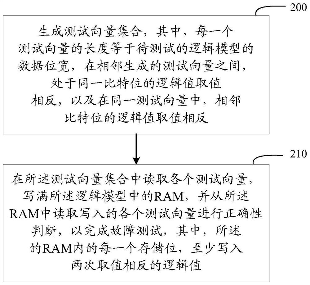
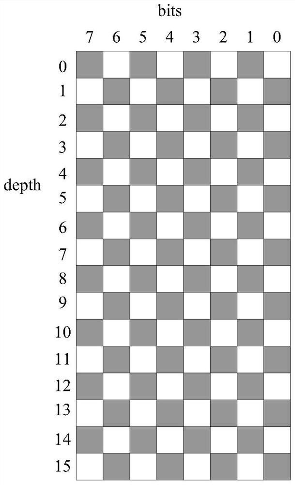
[0071] In order to improve the test efficiency and fault coverage of the logic model without occupying a large amount of logic resources, in the embodiment of the present invention, a set of test vectors is generated according to a preset checkerboard format, and is passed through the RAM in the logic model to be tested. Write and read the test vectors in the test vector set to complete the fault test of the RAM.

[0072] In this way, there is no need to download a separate test configuration file separately, and the built-in self-test for the logic model can be completed in the chip reset initialization stage, occupying less resources, and covering the main failure modes that can be generated by the logic model.

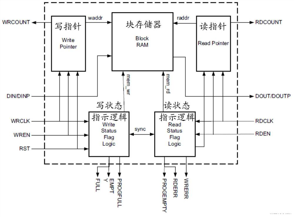
[0073] In the embodiment of the present invention, taking the logic model to be tested as an example of a FIFO model, the internal testing process of the FPGA chip is introduced in detail.

[0074] First of all, in the FIFO model, the read-write address of RAM is de...


PUM


Abstract

The invention relates to the chip technology, and in particular to a method and a device for testing a logical model in a chip for improving the test efficiency and the fault coverage of the logical model without occupying a large amount of logical resources. The method is as follows: generating a test vector set according to a preset checkerboard format, writing and reading test vectors in the test vector set from an RAM in a logical model to be tested so as to complete a fault test on the RAM, wherein each memory bit is read and written by using two logical values with opposite values in theRAM, so that RAM detection can be realized without reconfiguring an FPGA chip, and the adopted detection circuit is simple in structure, is easy to implement, and occupies fewer logical resources, sothat various types faults of the RAM in the logical model can be detected accurately and comprehensively without without occupying a large amount of logical resources, thereby improving the test efficiency and the fault coverage.

Description

technical field [0001] The invention relates to chip technology, in particular to a method and device for testing logic models in a chip. Background technique [0002] In the existing technology, there are a large number of first-in-first-out (Fisrt InFirst Out, FIFO) models in the data link in the digital communication baseband chip, which are used for flow control back pressure and cross-clock domain processing. The failure of the FIFO model will directly affect the communication Signal transmission, therefore, requires effective means to test the FIFO models in various chips. [0003] At present, the Field-Programmable Gate Array (FPGA) chip is a commonly used digital communication baseband chip. FPGA chip manufacturing is based on the Static Random Access Memory (SRAM) structure, which is flexible and configurable online. Its basic unit is composed of a look-up table (Look-UpTable, LUT), a register (Register), a random-access memory (Random-Access Memory, random-access ...

Claims


Application Information

Patent Timeline
Patent Type & Authority Patents(China)
IPC IPC(8): G11C29/00
CPCG01R31/31718
Inventor 徐红薇李硕董紫淼李增锴窦卢新谢立群
Owner DATANG MOBILE COMM EQUIP CO LTD
Why Eureka
Try Eureka