Double exposure method of nand flash memory structure

A double exposure and flash memory technology, which is applied in the manufacture of electrical components, circuits, semiconductors/solid-state devices, etc., can solve the problems of inaccurate size of the sacrificial layer and uneven etching of the structure

Active Publication Date: 2021-06-04
SHANGHAI HUALI MICROELECTRONICS CORP
View PDF10 Cites 0 Cited by
  • Summary
  • Abstract
  • Description
  • Claims
  • Application Information

AI Technical Summary

Problems solved by technology

like figure 1 As shown, the current method of double exposure process will cause the size of the sacrificial layer to be inaccurate, so that the shape of the sacrificial layer is prone to the problem of small top and large bottom, such as figure 2 As shown, in the subsequent etching process, the sacrificial layer with a small top and a large bottom will lead to uneven etching of the structure between the sacrificial layer substrate and the sacrificial layer

Method used


Image

  • Double exposure method of nand flash memory structure
  • Double exposure method of nand flash memory structure
  • Double exposure method of nand flash memory structure

Examples


Embodiment Construction

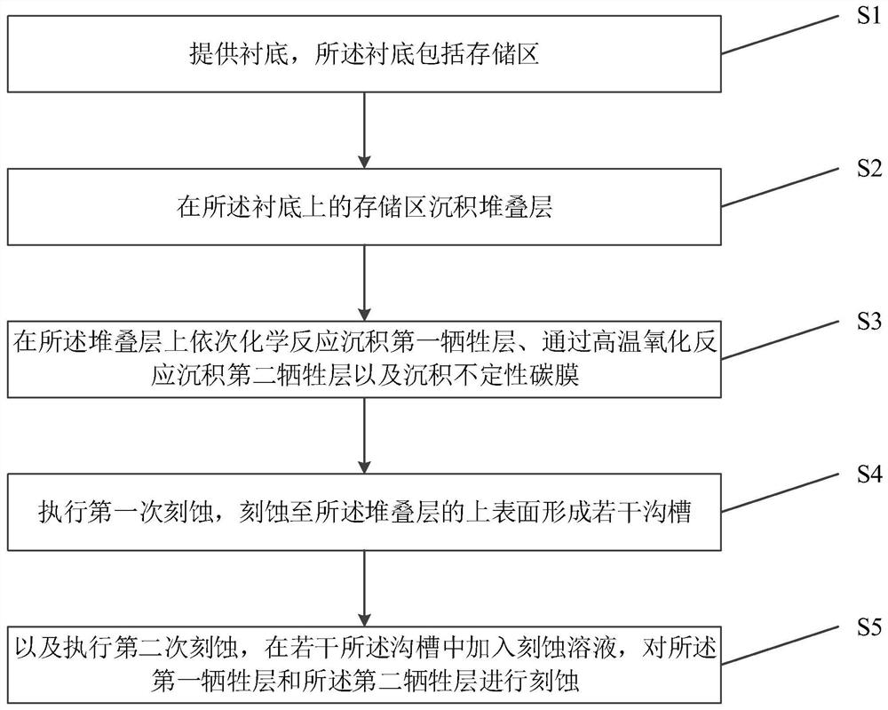
[0036] The specific implementation manner of the present invention will be described in more detail below with reference to schematic diagrams. Advantages and features of the present invention will be apparent from the following description and claims. It should be noted that all the drawings are in a very simplified form and use imprecise scales, and are only used to facilitate and clearly assist the purpose of illustrating the embodiments of the present invention.

[0037] In the following description, it will be understood that when a layer (or film), region, pattern or structure is referred to as being "on" a substrate, layer (or film), region and / or pattern, it can be directly on another layer or substrate, and / or intervening layers may also be present. Further, it will be understood that when a layer is referred to as being 'under' another layer, it can be directly under, and / or one or more intervening layers may also be present. In addition, designations regarding 'on...


PUM


Abstract

The invention provides a double exposure method of a NAND flash memory structure, comprising the following steps: providing a substrate, the substrate including a storage area; depositing stacked layers on the storage area on the substrate; successively depositing stacked layers on the stacked layers Depositing the first sacrificial layer by chemical reaction, depositing the second sacrificial layer by high temperature oxidation reaction and depositing the indeterminate carbon film; performing the first etching, etching to the upper surface of the stacked layer to form several grooves; performing the second For secondary etching, an etching solution is added to several of the trenches to etch the first sacrificial layer and the second sacrificial layer. And by using two sacrificial layers with different formation methods, the etching rate of the first sacrificial layer and the second sacrificial layer can be controlled during the second etching, so as to control the morphology of the first sacrificial layer and the second sacrificial layer As well as critical dimensions, thereby reducing the possibility of uneven etching in subsequent etching.

Description

technical field [0001] The invention relates to the field of semiconductors, in particular to a double exposure method for a NAND flash memory structure. Background technique [0002] NAND flash memory is mainly used to store data. Our commonly used flash memory products, such as flash drives and digital memory cards, all use NAND flash memory. NAND flash memory is a better storage solution than hard drives, especially in low-capacity applications up to 4GB. As people continue to pursue products that consume less power, weigh less and perform better, NAND flash is an attractive product. [0003] figure 1 is a photomicrograph of the barrier layer in the prior art, figure 2 Micrographs of etch non-uniformities appearing for subsequent etch in the prior art. In the prior art, for NAND flash memory with a process node of 40 nanometers and below, it is usually produced by a double exposure process, and a sacrificial layer with a size of 40 nanometers and below is obtained th...

Claims


Application Information

Patent Timeline
Patent Type & Authority Patents(China)
IPC IPC(8): H01L21/027
CPCH01L21/0274H01L21/0276
Inventor 何理巨晓华黄冠群
Owner SHANGHAI HUALI MICROELECTRONICS CORP
Why Eureka
Try Eureka