Vacuum device, attraction device, and conductive thin film manufacturing device

A technology of adsorption device and vacuum device, which is applied in semiconductor/solid-state device manufacturing, vacuum evaporation coating, and holding device for application of electrostatic attraction, etc. It can solve the problems that the film growth rate cannot be increased.

Active Publication Date: 2019-08-02
ULVAC INC
View PDF6 Cites 0 Cited by
  • Summary
  • Abstract
  • Description
  • Claims
  • Application Information

AI Technical Summary

Problems solved by technology

[0005] Therefore, there is, for example, a technique of attaching the back surface of a large substrate to a holding plate with an adhesive, and erecting the large substrate to form a thin film on the surface. However, since the adhesive is used, the upper limit of the temperature of the large substrate is The problem that the growth rate of the film cannot be increased due to low temperature

Method used


Image

  • Vacuum device, attraction device, and conductive thin film manufacturing device
  • Vacuum device, attraction device, and conductive thin film manufacturing device
  • Vacuum device, attraction device, and conductive thin film manufacturing device

Examples


Embodiment Construction

[0076] The present invention was conceived to solve the above-mentioned disadvantages of the prior art, and aims to provide a technique capable of stably growing a conductive film on a dielectric substrate.

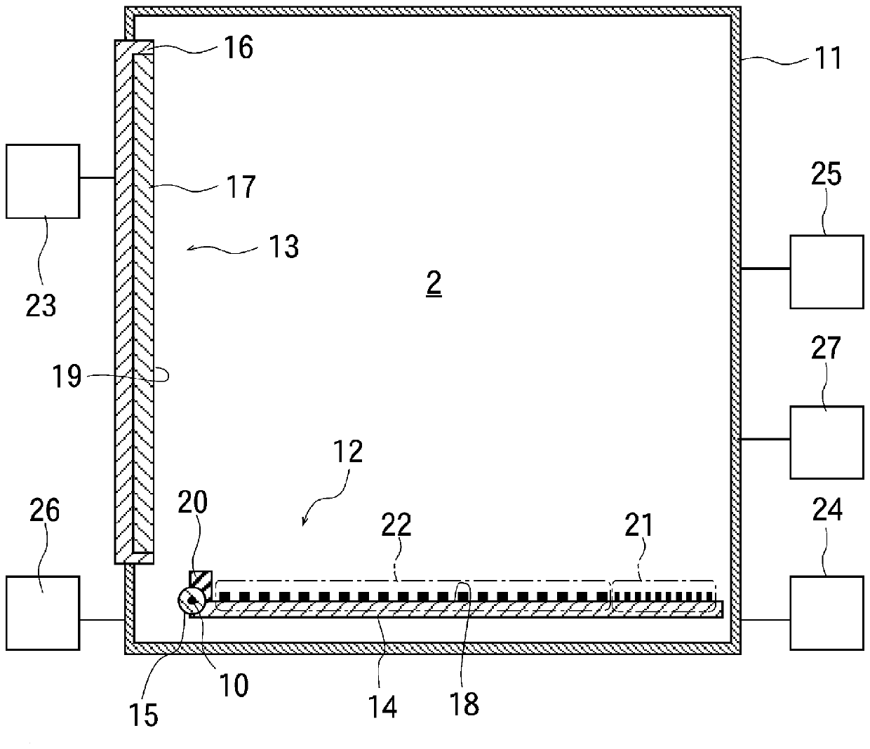
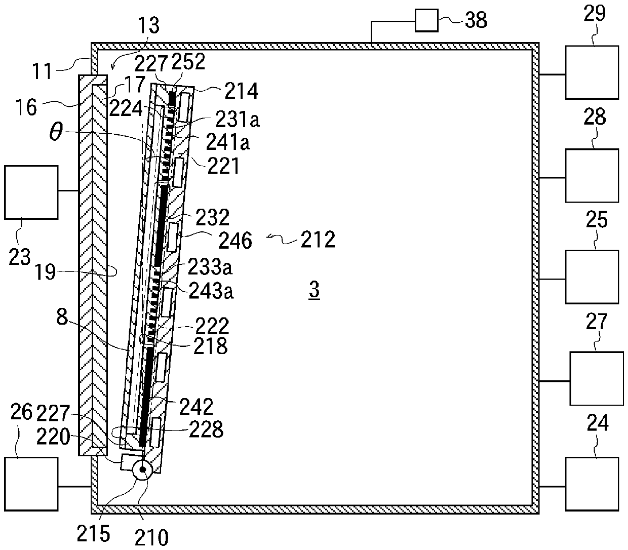
[0077] figure 1 The symbol 2 in the symbol 2 shows the vacuum device of the present invention, which has a vacuum chamber 11 , an adsorption device 12 and a target device 13 .

[0078] A rotating device 26 such as a motor and a sputtering power source 23 are disposed outside the vacuum chamber 11 .

[0079] The target device 13 has a sputtering target 17 to be sputtered and a cathode electrode 16 on which the sputtering target 17 is mounted, and the cathode electrode 16 is connected to a sputtering power supply 23 .

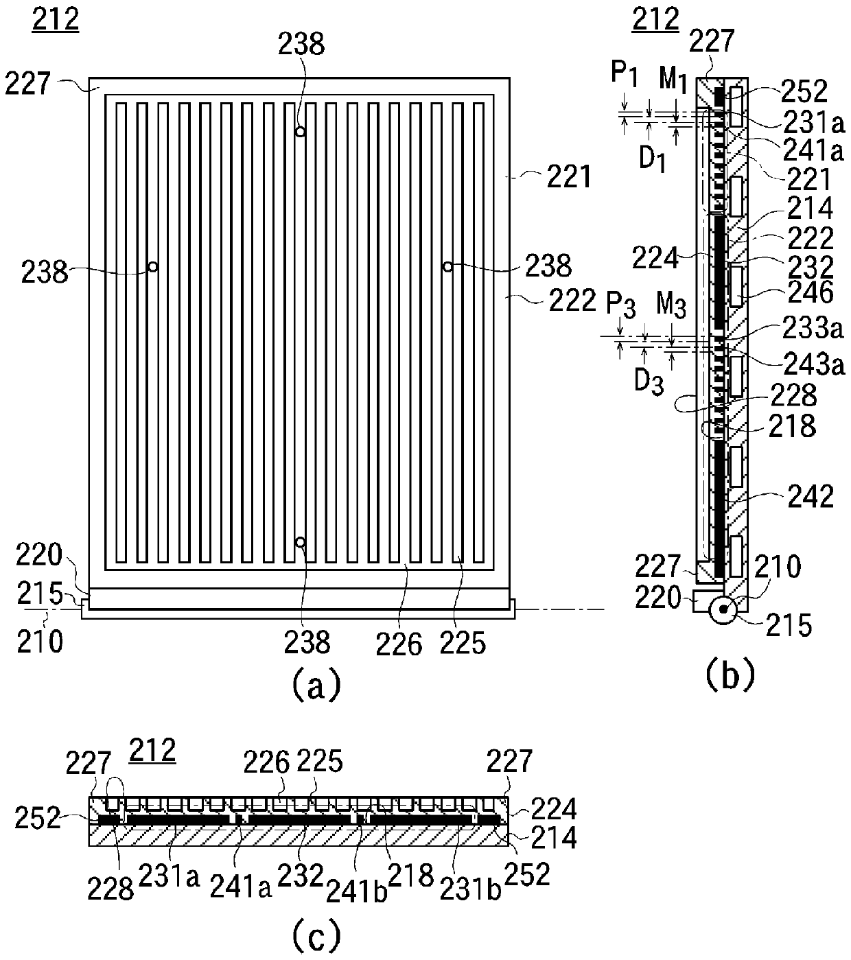
[0080] The adsorption device 12 has a rectangular or square adsorption plate 14 and a rod-shaped rotating shaft 15 arranged on one side of the adsorption plate 14. The rotating shaft 15 is connected to the rotating device 26, and the rotating shaft 15 rota...


PUM


Abstract

According to the present invention, a conductive thin film is grown while a dielectric object to be attracted is being erected. First positive and negative electrodes 31, 41 are placed in a first region 21 provided in the upper part of an attraction plate 14, while second positive and negative electrodes 32, 42, which have a greater width than the first positive and negative electrodes 31, 41 andwhich are laid at a greater interval than between the first positive and negative electrodes, are placed in a second region provided between a rotational axis line 10 and the first region 21. While the dielectric object is being attracted by a gradient force generated through application of a first voltage on the first positive and negative electrodes 31, 41, the attraction plate 14 is brought into an upright position from a horizontal position; and while a second voltage is being applied to the second positive and negative electrodes 32, 42, a conductive thin film is grown on the surface of the object 8 being attracted. In this configuration, the object 8 continues to be attracted, and thus will not fall off from the attraction plate 14. By introducing a heating medium gas between the object being attracted and the attraction plate 14 after attraction by an electrostatic force starts, the temperature of the object being attracted can be controlled.

Description

technical field [0001] The present invention relates to vacuum devices and in particular to adsorption devices for use in vacuum devices. Background technique [0002] In order to form a thin film on the surface of a large substrate in a state of high thermal conductivity by placing a large substrate horizontally on the adsorption device and adsorbing it, there is a method of attaching the electrode of the adsorption device to the back surface of the large substrate and applying a high voltage to the electrode to adsorb the large substrate. The technology of the substrate adsorption device uses an adsorption device that generates electrostatic force (also called electrostatic adsorption force) to adsorb a large substrate with a conductive film formed on the surface, and uses an electrostatic force that generates a gradient force to adsorb a large substrate composed of a dielectric. adsorption device. [0003] Display devices such as liquid crystal display devices have grown...

Claims


Application Information

Patent Timeline
Patent Type & Authority Applications(China)
IPC IPC(8): H01L21/683C23C14/50H01L21/285H02N13/00
CPCC23C14/34C23C14/50H01L21/285H01L21/683C23C14/228H01L21/2855H01L21/6833H02N13/00C23C14/505H01J37/32724
Inventor 前平谦不破耕橘高朋子大野哲宏阪上弘敏
Owner ULVAC INC
Why Eureka
Try Eureka