Organic electroluminescence material and organic electroluminescence device with material

An electroluminescent material and luminescent technology, applied in the direction of luminescent materials, electrical solid devices, electrical components, etc., can solve problems such as large tension, lower performance of organic electroluminescent devices, broken bonds, etc., to achieve enhanced thermal stability, Excellent hole transport performance, effect of lowering driving voltage

Active Publication Date: 2019-08-09
SHAANXI LIGHTE OPTOELECTRONICS MATERIAL CO LTD
View PDF13 Cites 9 Cited by
  • Summary
  • Abstract
  • Description
  • Claims
  • Application Information

AI Technical Summary

Problems solved by technology

However, the five-membered ring of fluorene in 9'9 diphenylfluorene is highly strained, and it is easy to break bonds at hi

Method used


Image

  • Organic electroluminescence material and organic electroluminescence device with material
  • Organic electroluminescence material and organic electroluminescence device with material
  • Organic electroluminescence material and organic electroluminescence device with material

Examples


Embodiment 1

[0162] Embodiment 1: red organic electroluminescent device

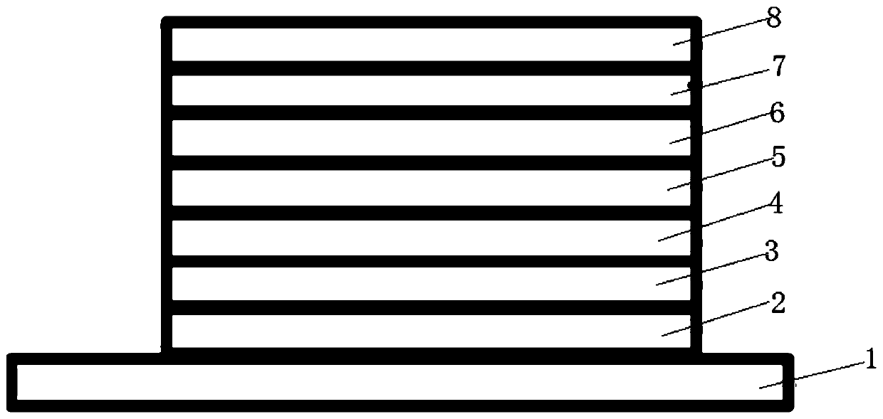
[0163] The anode was prepared by the following process: the thickness was The ITO substrate (manufactured by Corning) was cut into a size of 40mm × 40mm × 0.7mm, and it was prepared into an experimental substrate with cathode, anode and insulating layer patterns by using a photolithography process, using ultraviolet ozone and O 2 :N 2 Plasma surface treatment was performed to increase the work function of the anode (experimental substrate) and to remove scum.

[0164] Vacuum vapor-deposit m-MTDATA on the experimental substrate (anode) to form a thickness of The hole injection layer (HIL), and NPB is evaporated on the hole injection layer to form a thickness of The first hole transport layer (HT1).

[0165] Compound 1 was vacuum evaporated on the first hole transport layer to form a thickness of The second hole transport layer (HT2).

[0166] Evaporate 4,4'-N,N'-dicarbazole-biphenyl (referred to as "CBP") as...

Embodiment 6

[0183] Embodiment 6: blue organic electroluminescent device

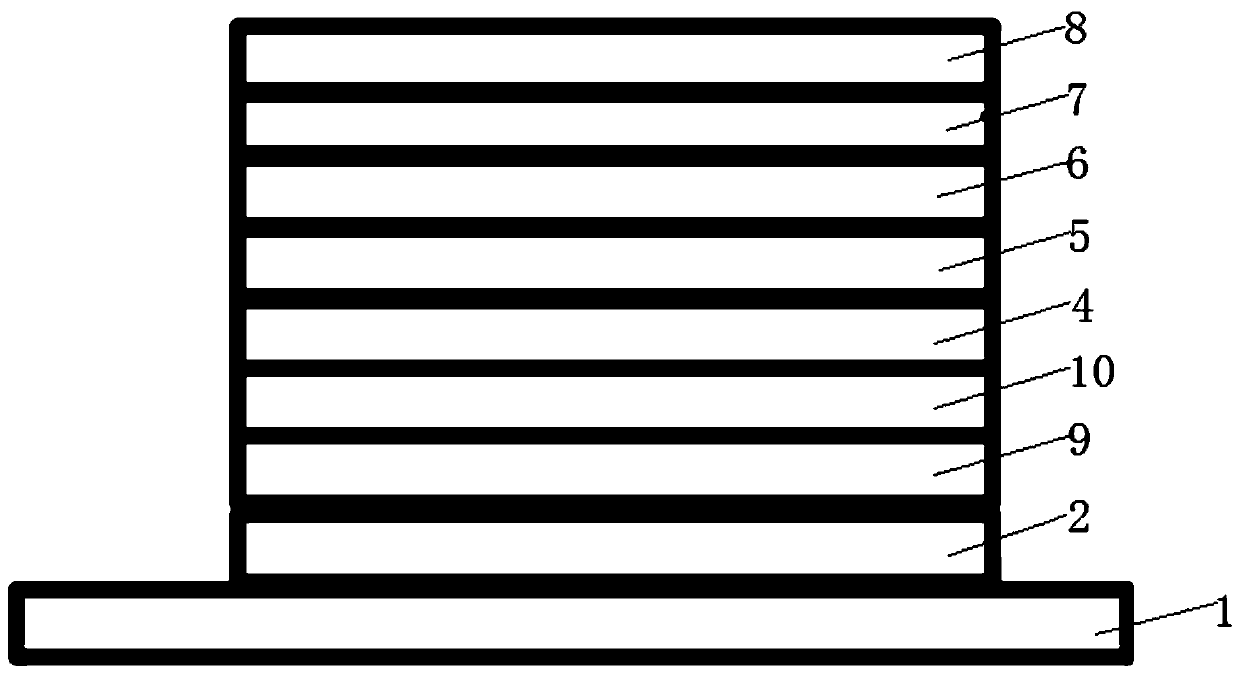
[0184] The anode was prepared by the following process: the thickness was The ITO substrate (manufactured by Corning) was cut into a size of 40mm × 40mm × 0.7mm, and it was prepared into an experimental substrate with cathode, anode and insulating layer patterns by using a photolithography process, using ultraviolet ozone and O 2 :N 2 Plasma surface treatment was performed to increase the work function of the anode (experimental substrate) and to remove scum.

[0185] Vacuum evaporated m-MTDATA on the experimental substrate (anode) to form a thickness of The hole injection layer (HIL), and the compound 6 is vacuum evaporated on the hole injection layer to form a thickness of The first hole transport layer (HT1).

[0186] Evaporate TCTA on the first hole transport layer to form a thickness of The second hole transport layer (HT2).

[0187] Using α,β-AND as the main body and doping 4,4'-(3,8-diphenylpyrene-1...

Embodiment 7-10

[0191] An organic electroluminescence device was fabricated by the same method as in Example 6, except that the compounds shown in Table 2 were each used when forming the first hole transport layer (HT1).

[0192] That is, Example 7 uses Compound 7 to make an organic electroluminescent device, Example 8 uses Compound 8 to make an organic electroluminescent device, Example 9 uses Compound 9 to make an organic electroluminescent device, and Example 10 uses Compound 10 to make an organic electroluminescent device. Light-emitting device, the device performance is shown in Table 2.


PUM


Abstract

The invention relates to an organic electroluminescence material and an organic electroluminescence device with the material. Novel aryl group-dihydrophenanthrene is introduced as one of core groups,a dihydrophenanthrene derivative is obtained and has high molecular weight, the glass transition temperature and decomposition temperature of the material can be increased, the heat stability of the material is improved, and the service life of the device is prolonged; the compound with the dihydrophenanthrene group has excellent hole transport capacity and can be applied to manufacturing of the organic electroluminescence device, used as a hole injection layer, a hole transport layer and the like in the organic electroluminescence device and particularly used as a hole transport layer material in the organic electroluminescence device, the secondary associativity of electronics and holes in an OLED device is improved, the driving voltage can be effectively lowered, the luminescence efficiency of the organic electroluminescence device is improved, and the service life of the organic electroluminescence device is prolonged.

Description

technical field [0001] The invention relates to the technical field of organic electroluminescent materials, in particular to an organic electroluminescent material and an organic electroluminescent device containing the material. Background technique [0002] In recent years, organic electroluminescent device (OLED: Organic electroluminescent device), as a new generation of display technology, has gradually entered people's field of vision. A common organic electroluminescent device is composed of an anode, a cathode, and more than one organic layer arranged between the cathode and the anode. When a voltage is applied to the cathode and anode, the two electrodes generate an electric field. Under the action of the electric field, the electrons on the cathode side move to the light-emitting layer, and the electrons on the anode side also move to the light-emitting layer. The two combine to form excitons in the light-emitting layer, and the excitons are excited. The state rel...

Claims


Application Information

Patent Timeline
IPC IPC(8): C07C211/54C07C211/58C07C211/61C07D209/88C07D307/91C07D333/76C07D405/12C07D409/12C07F7/08C09K11/06H01L51/54H01L51/50
CPCC07C211/61C07D209/88C07D307/91C07D333/76C07D405/12C07D409/12C07C211/54C07C211/58C07F7/081C09K11/06C09K2211/1011C09K2211/1014C09K2211/1029C09K2211/1088C09K2211/1092C07C2603/18C07C2603/26C07C2603/94H10K85/615H10K85/624H10K85/631H10K85/636H10K85/626H10K85/633H10K85/6574H10K85/6576H10K85/40H10K85/6572H10K50/156
Inventor 马天天冯震李红燕李健沙荀姗
Owner SHAANXI LIGHTE OPTOELECTRONICS MATERIAL CO LTD
Why Eureka
Try Eureka