Multi-layer photocurable resin comprehensive covering package method for organic electronic device

A technology of organic electronic devices and photocurable resins, applied in the direction of electric solid devices, electrical components, semiconductor devices, etc., can solve the problems of slow production speed, complex structure, many steps, etc., to reduce the process cost, improve the coating rate, Reduce the effect of etching

Pending Publication Date: 2019-08-20
NANJING FLEXIBLE MATERIALS CO LTD
View PDF6 Cites 5 Cited by
  • Summary
  • Abstract
  • Description
  • Claims
  • Application Information

AI Technical Summary

Problems solved by technology

[0006] The purpose of the present invention is to provide a method for encapsulating organic electronic devices with multi-layer photocurable resin to fully cover the encapsulation, so as to overcome the problems of complex structure, many steps, high cost and slow production speed in the current organic encapsulation structure

Method used


Image

  • Multi-layer photocurable resin comprehensive covering package method for organic electronic device

Examples


Embodiment Construction

[0038] Specific embodiments of the present invention are described in detail below, but it should be understood that the protection scope of the present invention is not limited by the specific embodiments.

[0039] Unless expressly stated otherwise, throughout the specification and claims, the term "comprise" or variations thereof such as "includes" or "includes" and the like will be understood to include the stated elements or constituents, and not Other elements or other components are not excluded.

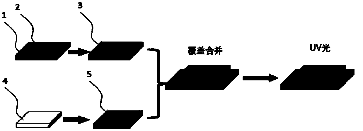
[0040] According to the design and process of the invention, its packaging scheme is very simple and practical, and the following steps are adopted:

[0041] The first step is to prepare the glass or high-barrier flexible PET substrate, and the surface can be cleaned. And put it into a vacuum drying oven to remove more than adsorbed water vapor and oxygen. Put glass or high-barrier flexible PET substrates into organic light-emitting diode devices to grow and prepare OLED dev...


PUM


Abstract

The invention discloses a multi-layer photocurable resin comprehensive covering package method for an organic electronic device. The method comprises a step of transferring a sample into a nitrogen glove box and applying an inert UV curing protective adhesive on an organic device, a step of applying a high-water-oxygen barrier UV curing adhesive on glass or flexible cover plate (high water-oxygenbarrier film) in the nitrogen glove box, covering the sample with a package covering layer with the completion of application, and smoothing and pressing, and a step of placing the device under a UV lamp to cure to complete packaging and bonding. Compared with the prior art, the present invention has the following advantages that the packaging process and materials consider the protection of the device, at the same time, the package is completed as quickly as possible, and the risk of device damage is reduced. During the packaging process, a package layer can completely cover the device, and the steps of etching, positioning and printing are reduced. In this way, the device can be protected from accidental damage, the application rate can be reduced, and the process cost is reduced.

Description

technical field [0001] The invention belongs to the technical field of organic electronic device encapsulation research, and in particular relates to an organic electronic device encapsulation multi-layer light-curable resin comprehensive covering encapsulation method. Background technique [0002] New organic electronic devices, organic light emitting devices, organic optoelectronic devices, organic detectors and organic field effect tubes are widely used in display and solid-state lighting, energy sources, detectors, mobile phones, wearables, etc. The field has broad application prospects. Its excellent characteristics will affect the development of next-generation display electronics, and it is the main force of flexible electronic displays. [0003] However, according to a long-term, a large number of organic electronics studies have shown that the water vapor and oxygen components in the air have a fatal impact on organic electronic devices. The main reason is that wat...

Claims


Application Information

Patent Timeline
Patent Type & Authority Applications(China)
IPC IPC(8): H01L51/40H01L51/48H01L51/56H01L51/10H01L51/44H01L51/52
CPCH10K71/00H10K10/88H10K30/88H10K50/844Y02E10/549
Inventor 林群
Owner NANJING FLEXIBLE MATERIALS CO LTD
Why Eureka
Try Eureka